


 The Marketing Minute: Cracking the Code of Technical Marketing
 Trouble in Your Tank: Implementing Direct Metallization in Advanced Substrate Packaging


Printed Sensors Monitor Tire Wear in Real Time
June 20, 2017 | Duke UniversityEstimated reading time: 4 minutes
Electrical engineers at Duke University have invented an inexpensive printed sensor that can monitor the tread of car tires in real time, warning drivers when the rubber meeting the road has grown dangerously thin.
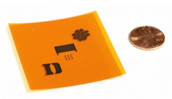
A demonstration of the printed carbon nanotubes on a flexible surface. The prototype tire tread sensor (middle) is flanked by the logos of Duke University and Fetch Automotive Design Group.
If adopted, the device will increase safety, improve vehicle performance and reduce fuel consumption. The group hopes that the tire wear sensor will be the first of many that could disrupt the $2 billion tire and wheel control sensor market.
In collaboration with Fetch Automotive Design Group, the Duke researchers have demonstrated a design using metallic carbon nanotubes (tiny cylinders of carbon atoms just one-billionth of a meter in diameter) that can track millimeter-scale changes in tread depth with 99 percent accuracy. With two patents pending, the researchers are in the process of establishing industry collaborations to bring the technology to a tire near you.
"With all of the technology and sensors that are in today's cars, it's kind of crazy to think that there's almost no data being gathered from the only part of the vehicle that is actually touching the road," said Aaron Franklin, associate professor of electrical and computer engineering at Duke. "Our tire tread sensor is the perfect marriage between high-end technology and a simple solution."
An illustration of how the novel tread sensor works. The sensor is placed on the inside of the tire, where the tire wall and tread interferes with an electric field that arcs between two electrodes. That interference can be measured to determine the thickness of the rubber with millimeter accuracy.
The technology relies on the well-understood mechanics of how electric fields interact with metallic conductors. The core of the sensor is formed by placing two small, electrically conductive electrodes very close to each other. By applying an oscillating electrical voltage to one and grounding the other, an electric field forms between the electrodes.
While most of this electric field passes directly between the two electrodes, some of the field arcs between them. When a material is placed on top of the electrodes, it interferes with this so-called "fringing field." By measuring this interference through the electrical response of the grounded electrode, it is possible to determine the thickness of the material covering the sensor.
While there is a limit to how thick a material this setup can detect, it is more than enough to encompass the several millimeters of tread found in today's tires. And with evidence of sub-millimeter resolution, the technology could easily tell drivers when it's time to buy a new set of tires or give information about uneven and often dangerous tire wear by connecting many sensors in a grid to cover the width of the tire.
Tests also proved that the metal mesh embedded within tires does not disrupt the operation of the new sensors.
"When we pitch this idea to industry experts, they say to each other, 'Why haven't we tried that before?'" said Franklin. "It seems so obvious once you see it, but that's the way it is with most good inventions."
While the sensor could be made from a variety of materials and methods, the paper explains how the researchers optimized performance by exploring different variables from sensor size and structure to substrate and ink materials. The best results were obtained by printing electrodes made of metallic carbon nanotubes on a flexible polyimide film. Besides providing the best results, the metallic carbon nanotubes are durable enough to survive the harsh environment inside a tire.
The sensors can be printed on most anything using an aerosol jet printer -- even on the inside of the tires themselves. And, while it is not yet certain that direct printing will be the best manufacturing approach, whatever approach is ultimately used, Franklin said the sensors should cost far less than a penny apiece once they're being made in quantity.
Franklin's group also wants to explore other automotive applications for the printed sensors, such as keeping tabs on the thickness of brake pads or the air pressure within tires. This is consistent with a key trend in the automotive sector toward using embedded nanosensors.
Other tire tracking products have recently hit the market. For example, the tire company Pirelli recently unveiled a system to electronically track each tire -- when it was installed, how many miles it has gone, when it was last serviced, etc. -- and use an algorithm to estimate its wear and tear. While not the same thing as actively, physically measuring tire tread, it shows that the market is there for this type of information.
But the technology isn't limited to cars.
"This setup could be used with just about anything that isn't metallic or too thick," said Franklin. "Right now we're focusing on tires, but really anything you'd rather not have to cut apart to determine its thickness could be monitored by this technology in real time."
"Noninvasive Material Thickness Detection by Aerosol Jet Printed Sensors Enhanced Through Metallic Carbon Nanotube Ink," Joseph B. Andrews, Changyong Cao, Martin A. Brooke and Aaron D. Franklin. IEEE Sensors Journal, June 5, 2017. DOI: 10.1109/JSEN.2017.2710085
Share on:


Testimonial
"The I-Connect007 team is outstanding—kind, responsive, and a true marketing partner. Their design team created fresh, eye-catching ads, and their editorial support polished our content to let our brand shine. Thank you all! "
Sweeney Ng - CEE PCBSuggested Items
Curing and Verification in PCB Shadow Areas
09/17/2025 | Doug Katze, DymaxDesign engineers know a simple truth that often complicates electronics manufacturing: Light doesn’t go around corners. In densely populated PCBs, adhesives and coatings often fail to fully cure in shadowed regions created by tall ICs, connectors, relays, and tight housings.
Altair, Wichita State University’s NIAR Sign MoU to Accelerate Aerospace Innovation
09/16/2025 | AltairAltair, a global leader in computational intelligence, and Wichita State University’s (WSU) National Institute for Aviation Research (NIAR), one of the world’s leading aerospace research institutions, have signed a memorandum of understanding (MoU) to advance innovation across the aerospace and defense industries.
AI-Powered Wearables Transform How Consumers Interact with Everyday Technology
09/15/2025 | PR NewswireThe global demand for AI-driven, touchless wearable technologies is accelerating as consumers seek more natural, seamless and intuitive ways to interact with their devices. Traditional touch screens and voice assistants, while effective, are increasingly viewed as limiting in a world where multitasking, mobility and efficiency are key. As industries from consumer electronics to augmented reality and enterprise computing embrace the possibilities of gesture-based control, the market for neural interfaces is rapidly expanding
Hanwha Aerospace to Collaborate with BAE Systems on Advanced Anti-jamming GPS for Guided Missiles
09/15/2025 | HanwhaHanwha Aerospace has signed a contract with BAE Systems to integrate next-generation, anti-jamming Global Positioning System (GPS) technology into Hanwha Aerospace’s Deep Strike Capability precision-guided weapon system.
United Electronics Corporation Unveils Revolutionary CIMS Galaxy 30 Automated Optical Inspection System
09/11/2025 | United Electronics CorporationUnited Electronics Corporation (UEC) today announced the launch of its new groundbreaking CIMS Galaxy 30 Automated Optical Inspection (AOI) machine, setting a new industry standard for precision electronics manufacturing quality control. The Galaxy 30, developed and manufactured by CIMS, represents a significant leap forward in inspection technology, delivering exceptional speed improvements and introducing cutting-edge artificial intelligence capabilities.