


 The Marketing Minute: Cracking the Code of Technical Marketing
 Trouble in Your Tank: Implementing Direct Metallization in Advanced Substrate Packaging


'Magic' Alloy Could Spur Next Generation of Solar Cells
June 20, 2017 | University of MichiganEstimated reading time: 4 minutes
In what could be a major step forward for a new generation of solar cells called "concentrator photovoltaics," University of Michigan researchers have developed a new semiconductor alloy that can capture the near-infrared light located on the leading edge of the visible light spectrum.
Easier to manufacture and at least 25% less costly than previous formulations, it's believed to be the world's most cost-effective material that can capture near-infrared light—and is compatible with the gallium arsenide semiconductors often used in concentrator photovoltaics.
Concentrator photovoltaics gather and focus sunlight onto small, high-efficiency solar cells made of gallium arsenide or germanium semiconductors. They're on track to achieve efficiency rates of over 50%, while conventional flat-panel silicon solar cells top out in the mid-20s.
"Flat-panel silicon is basically maxed out in terms of efficiency," said Rachel Goldman, U-M professor of materials science and engineering, and physics, whose lab developed the alloy. "The cost of silicon isn't going down and efficiency isn't going up. Concentrator photovoltaics could power the next generation."
Varieties of concentrator photovoltaics exist today. They are made of three different semiconductor alloys layered together. Sprayed onto a semiconductor wafer in a process called molecular-beam epitaxy—a bit like spray painting with individual elements—each layer is only a few microns thick. The layers capture different parts of the solar spectrum; light that gets through one layer is captured by the next.
But near-infrared light slips through these cells unharnessed. For years, researchers have been working toward an elusive "fourth layer" alloy that could be sandwiched into cells to capture this light. It's a tall order; the alloy must be cost-effective, stable, durable and sensitive to infrared light, with an atomic structure that matches the other three layers in the solar cell.
Getting all those variables right isn't easy, and until now, researchers have been stuck with prohibitively expensive formulas that use five elements or more.
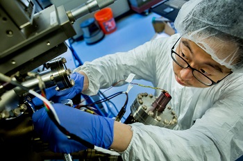
The main growth chamber of the molecular epitaxy beam apparatus in which members of MSE Professor Rachel Goodman's research group characterize various semiconductors in the Gerstacker Building on August 3, 2015. Photo Credit: Joseph XuTo find a simpler mix, Goldman's team devised a novel approach for keeping tabs on the many variables in the process. They combined on-the-ground measurement methods including X-ray diffraction done at U-M and ion beam analysis done at Los Alamos National Laboratory with custom-built computer modeling.
Using this method, they discovered that a slightly different type of arsenic molecule would pair more effectively with the bismuth. They were able to tweak the amount of nitrogen and bismuth in the mix, enabling them to eliminate an additional manufacturing step that previous formulas required. And they found precisely the right temperature that would enable the elements to mix smoothly and stick to the substrate securely.
"'Magic' is not a word we use often as materials scientists," Goldman said. "But that's what it felt like when we finally got it right."
The advance comes on the heels of another innovation from Goldman's lab that simplifies the "doping" process used to tweak the electrical properties of the chemical layers in gallium arsenide semiconductors. During doping, manufacturers apply a mix of chemicals called "designer impurities" to change how semiconductors conduct electricity and give them positive and negative polarity similar to the electrodes of a battery. The doping agents usually used for gallium arsenide semiconductors are silicon on the negative side and beryllium on the positive side.
The beryllium is a problem—it's toxic and it costs about 10 times more than silicon dopants. Beryllium is also sensitive to heat, which limits flexibility during the manufacturing process. But the U-M team discovered that by reducing the amount of arsenic below levels that were previously considered acceptable, they can "flip" the polarity of silicon dopants, enabling them to use the cheaper, safer element for both the
positive and negative sides.
"Being able to change the polarity of the carrier is kind of like atomic 'ambidexterity,'" said Richard Field, a former U-M doctoral student who worked on the project. "Just like people with naturally born ambidexterity, it's fairly uncommon to find atomic impurities with this ability."
Together, the improved doping process and the new alloy could make the semiconductors used in concentrator photovoltaics as much as 30% cheaper to produce, a big step toward making the high-efficiency cells practical for large-scale electricity generation.
"Essentially, this enables us to make these semiconductors with fewer atomic spray cans, and each can is significantly less expensive," Goldman said. "In the manufacturing world, that kind of simplification is very significant. These new alloys and dopants are also more stable, which gives makers more flexibility as the semiconductors move through the manufacturing process."
The new alloy is detailed in a paper titled "Bi-enhanced N incorporation in GaAsNBi alloys," published June 15 in Applied Physics Letters. The research is supported by the National Science Foundation and the U.S. Department of Energy Office of Science Graduate Student Research.
The doping advances are detailed in a paper titled "Influence of surface reconstruction on dopant incorporation and transport properties of GaAs(Bi) alloys." It was published in the Dec. 26, 2016, issue of Applied Physics Letters. The research was supported by the National Science Foundation.
Share on:


Testimonial
"We’re proud to call I-Connect007 a trusted partner. Their innovative approach and industry insight made our podcast collaboration a success by connecting us with the right audience and delivering real results."
Julia McCaffrey - NCAB GroupSuggested Items
Alternative Manufacturing, Inc. (AMI) Announces Commitment to Excellence in Industrial, Defense, Aerospace, Renewables, and Robotics Markets
09/16/2025 | Alternative Manufacturing, Inc.Alternative Manufacturing, Inc. (AMI), a 100% employee-owned contract manufacturer, proudly reaffirms its leadership in the electronics manufacturing services (EMS) industry with a continued commitment to delivering high-quality PCBAs and box builds across the industrial, defense, aerospace, renewable energy, and robotics markets.
Sustainability and Selective Soldering
09/15/2025 | Dr. Samuel J. McMaster, Pillarhouse InternationalSustainability is more than just a buzzword for the electronics industry; it’s a key goal for all manufacturing processes. This is more than a box-ticking exercise or simply doing a small part for environmentally friendly processes. Moving toward sustainable solutions drives innovation and operational efficiency.
Trouble in Your Tank: Implementing Direct Metallization in Advanced Substrate Packaging
09/15/2025 | Michael Carano -- Column: Trouble in Your TankDirect metallization systems based on conductive graphite are gaining popularity throughout the world. The environmental and productivity gains achievable with this process are outstanding. Direct metallization reduces the costs of compliance, waste treatment, and legal issues related to chemical exposure. A graphite-based direct plate system has been devised to address these needs.
EV Group Achieves Breakthrough in Hybrid Bonding Overlay Control for Chiplet Integration
09/12/2025 | EV GroupEV Group (EVG), a leading provider of innovative process solutions and expertise serving leading-edge and future semiconductor designs and chip integration schemes, today unveiled the EVG®40 D2W—the first dedicated die-to-wafer overlay metrology platform to deliver 100 percent die overlay measurement on 300-mm wafers at high precision and speeds needed for production environments. With up to 15X higher throughput than EVG’s industry benchmark EVG®40 NT2 system designed for hybrid wafer bonding metrology, the new EVG40 D2W enables chipmakers to verify die placement accuracy and take rapid corrective action, improving process control and yield in high-volume manufacturing (HVM).
Integrating Uniplate PLBCu6 With the Digital Factory Suite
09/12/2025 | Giovanni Obino and Andreas Schatz, MKS' AtotechPrinted circuit board manufacturing is rapidly changing, driven by miniaturization, stringent reliability requirements, and growing pressure for sustainable production. Meeting these challenges requires more than incremental improvements; it demands a combination of precise equipment and real-time process intelligence. The pairing of Uniplate® PLBCu6 with the Digital Factory Suite (DFS) demonstrates how hardware and software can work together to create more responsive, resource-efficient manufacturing.