


 The Chemical Connection: Surface Finishes for PCBs
 It’s Only Common Sense: 7 Tips to Focus on What Works
 The Marketing Minute: Go Big or Go Home—Long-form Content Is Your Brand’s Best Friend


Akrometrix Launches New Warpage Metrology System
June 29, 2017 | Akrometrix LLCEstimated reading time: 1 minute
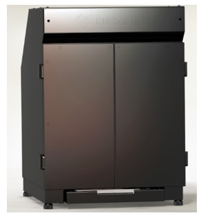
Akrometrix, LLC, the leading provider of thermal warpage and strain metrology equipment to both the front- and back-end semiconductor and electronics industries, is pleased to announce that it has launched its newest warpage metrology system – the Tabletop Shadow Moiré (TTSM) system.
“Over the years, many of our customers who are using our systems for thermal warpage metrology have stated a need for an ultra-fast, highly accurate room temperature warpage metrology system,” stated Mayson Brooks, Akrometrix President. “Additionally, they wanted a system that was small enough for a tabletop operation and that would allow them to utilize all the software features of our thermal warpage systems, only at room temperature.”
The TTSM meets this demand – enabling customers to measure warpage of substrates up to 300mm x 310 mm (a 300mm wafer or two JEDEC trays) with the entire measurement taking less than two seconds. Whether individual parts or a JEDEC tray of multiple parts, the TTSM provides an ultra-fast and highly accurate measurement at room temperature that is suited for tabletop use.
About Akrometrix LLC
Akrometrix is the leader in thermal warpage and strain metrology for the front-end/back-end wafer, back-end packaging/assembly, panel and the PCB/component markets. The company provides both capital equipment and test services to measure warpage and strain in temperatures from -50°C to 300°C on virtually any substrate up to 600mm x 600mm, regardless of shape. Located in Atlanta, Georgia, Akrometrix has been serving customers worldwide for more than 20 years based on technology developed at Georgia Tech. For more information click here.
Share on:


Suggested Items
Molex Releases New Report on Strategies for Advancing Rugged, Reliable Connectivity in Modern Aerospace and Defense Applications
04/01/2025 | MolexMolex, a global electronics leader and connectivity innovator, has released a new report from AirBorn, a Molex company, which explores the unrelenting demands for constant, continuous connectivity to support the rigors of modern aerospace, defense and space-industry applications.
Yamaha Reveals Latest Updates Boosting Ease of Use in 1 STOP SMART SOLUTION
04/01/2025 | Yamaha Robotics SMT SectionYamaha Robotics SMT Section has announced automated programming capabilities in YSUP factory software that streamline program generation for all surface-mount processes, including dispensing, printing, placement, and inspection.
Airbus to Design and Build ESA’s ExoMars Rover Lander Platform
03/31/2025 | AirbusAirbus has been selected by the European Space Agency (ESA) and Thales Alenia Space (TAS - a joint venture between Thales (67%) and Leonardo (33%)), the ExoMars industrial prime contractor, to build key systems for the ExoMars lander that will safely place the Rosalind Franklin rover on the surface of the Red Planet.
New Cryostatic Systems Elevate Current Research on Qubits
03/31/2025 | Fraunhofer IAFThe Center Nanoelectronic Technologies (CNT) at Fraunhofer IPMS has recently acquired new cryostats for the research on qubits and the qualification of superconducting systems.
The Knowledge Base: At the Forefront of Electronics Manufacturing
03/26/2025 | Mike Konrad -- Column: The Knowledge BaseThe electronics manufacturing industry is at a transformative crossroads, shaped by emerging technologies, shifting supply chain dynamics, sustainability initiatives, and the relentless push for miniaturization and efficiency. The industry's future will be defined by innovations in semiconductor manufacturing, automation, artificial intelligence (AI), and sustainable practices. Here, I will explore the key developments that are propelling the industry forward and their implications for manufacturers, engineers, and stakeholders.