


 The Marketing Minute: Cracking the Code of Technical Marketing
 Trouble in Your Tank: Implementing Direct Metallization in Advanced Substrate Packaging


Nanostructures Detect Colors
June 30, 2017 | CaltechEstimated reading time: 3 minutes
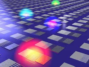
Engineers at Caltech have for the first time developed a light detector that combines two disparate technologies—nanophotonics, which manipulates light at the nanoscale, and thermoelectrics, which translates temperature differences directly into electron voltage—to distinguish different wavelengths of light, including both visible and infrared wavelengths, at high resolution.
Light detectors that distinguish between different colors of light or heat are used in a variety of applications, including satellites that study changing vegetation and landscape on the earth and medical imagers that distinguish between healthy and cancerous cells based on their color variations.
The new detector, described in a paper in Nature Nanotechnology on May 22, operates about 10 to 100 times faster than current comparable thermoelectric devices and is capable of detecting light across a wider range of the electromagnetic spectrum than traditional light detectors. In traditional light detectors, incoming photons of light are absorbed in a semiconductor and excite electrons that are captured by the detector. The movement of these light-excited electrons produces an electric current—a signal—that can be measured and quantified. While effective, this type of system makes it difficult to "see" infrared light, which is made up of lower-energy photons than those in visible light.
Because the new detectors are potentially capable of capturing infrared wavelengths of sunlight and heat that cannot be collected efficiently by conventional solar materials, the technology could lead to better solar cells and imaging devices.
"In nanophotonics, we study the way light interacts with structures that are much smaller than the optical wavelength itself, which results in extreme confinement of light. In this work, we have combined this attribute with the power conversion characteristics of thermoelectrics to enable a new type of optoelectronic device," says Harry Atwater, corresponding author of the study. Atwater is the Howard Hughes Professor of Applied Physics and Materials Science in the Division of Engineering and Applied Science at Caltech, and director of the Joint Center for Artificial Photosynthesis (JCAP). JCAP is a Department of Energy (DOE) Energy Innovation Hub focused on developing a cost-effective method of turning sunlight, water, and carbon dioxide into fuel. It is led by Caltech with Berkeley Lab as a major partner.
Atwater's team built materials with nanostructures that are hundreds of nanometers wide—smaller even than the wavelengths of light that represent the visible spectrum, which ranges from about 400 to 700 nanometers.
The researchers created nanostructures with a variety of widths, that absorb different wavelengths—colors—of light. When these nanostructures absorb light, they generate an electric current with a strength that corresponds to the light wavelength that is absorbed.
The detectors were fabricated in the Kavli Nanoscience Institute cleanroom at Caltech, where the team created subwavelength structures using a combination of vapor deposition (which condenses atom-thin layers of material on a surface from an element-rich mist) and electron beam lithography (which then cuts nanoscale patterns in that material using a focused beam of electrons). The structures, which resonate and generate a signal when they absorb photons with specific wavelengths, were created from alloys with well-known thermoelectric properties, but the research is applicable to a wide range of materials, the authors say.
"This research is a bridge between two research fields, nanophotonics and thermoelectrics, that don't often interact, and creates an avenue for collaboration," says graduate student Kelly Mauser (MS '16), lead author of the Nature Nanotechnology study. "There is a plethora of unexplored and exciting application and research opportunities at the junction of these two fields."
Share on:


Testimonial
"In a year when every marketing dollar mattered, I chose to keep I-Connect007 in our 2025 plan. Their commitment to high-quality, insightful content aligns with Koh Young’s values and helps readers navigate a changing industry. "
Brent Fischthal - Koh YoungSuggested Items
Curing and Verification in PCB Shadow Areas
09/17/2025 | Doug Katze, DymaxDesign engineers know a simple truth that often complicates electronics manufacturing: Light doesn’t go around corners. In densely populated PCBs, adhesives and coatings often fail to fully cure in shadowed regions created by tall ICs, connectors, relays, and tight housings.
Marcy’s Musings: Advancing the Advanced Materials Discussion
09/17/2025 | Marcy LaRont -- Column: Marcy's MusingsAs the industry’s most trusted global source of original content about the electronics supply chain, we continually ask you about your concerns, what you care about, and what you most want to learn about. Your responses are insightful and valuable. Thank you for caring enough to provide useful feedback and engage in dialogue.
September 2025 PCB007 Magazine: The Future of Advanced Materials
09/16/2025 | I-Connect007 Editorial TeamMoore’s Law is no more, and the advanced material solutions being developed to grapple with this reality are surprising, stunning, and perhaps a bit daunting. Buckle up for a dive into advanced materials and a glimpse into the next chapters of electronics manufacturing.
I-Connect007 Launches Advanced Electronics Packaging Digest
09/15/2025 | I-Connect007I-Connect007 is pleased to announce the launch of Advanced Electronics Packaging Digest (AEPD), a new monthly digital newsletter dedicated to one of the most critical and rapidly evolving areas of electronics manufacturing: advanced packaging at the interconnect level.
Panasonic Industry will Double the Production Capacity of MEGTRON Multi-layer Circuit Board Materials Over the Next Five Years
09/15/2025 | Panasonic Industry Co., Ltd.Panasonic Industry Co., Ltd., a Panasonic Group company, announced plans for a major expansion of its global production capacity for MEGTRON multi-layer circuit board materials today. The company plans to double its production over the next five years to meet growing demand in the AI server and ICT infrastructure markets.