


 The Marketing Minute: Cracking the Code of Technical Marketing
 Trouble in Your Tank: Implementing Direct Metallization in Advanced Substrate Packaging


Scientists Produce Dialysis Membrane Made From Graphene
June 30, 2017 | MITEstimated reading time: 4 minutes
Dialysis, in the most general sense, is the process by which molecules filter out of one solution, by diffusing through a membrane, into a more dilute solution. Outside of hemodialysis, which removes waste from blood, scientists use dialysis to purify drugs, remove residue from chemical solutions, and isolate molecules for medical diagnosis, typically by allowing the materials to pass through a porous membrane.
Today’s commercial dialysis membranes separate molecules slowly, in part due to their makeup: They are relatively thick, and the pores that tunnel through such dense membranes do so in winding paths, making it difficult for target molecules to quickly pass through.
Now MIT engineers have fabricated a functional dialysis membrane from a sheet of graphene — a single layer of carbon atoms, linked end to end in hexagonal configuration like that of chicken wire. The graphene membrane, about the size of a fingernail, is less than 1 nanometer thick. (The thinnest existing memranes are about 20 nanometers thick.) The team’s membrane is able to filter out nanometer-sized molecules from aqueous solutions up to 10 times faster than state-of-the-art membranes, with the graphene itself being up to 100 times faster.
1) Graphene, grown on copper foil, is pressed against a supporting sheet of polycarbonate. 2) The polycarbonate acts to peel the graphene from the copper. 3) Using interfacial polymerization, researchers seal large tears and defects in graphene. 4) Next, they use oxygen plasma to etch pores of specific sizes in graphene. Courtesy of the researchers (edited by MIT News)
While graphene has largely been explored for applications in electronics, Piran Kidambi, a postdoc in MIT’s Department of Mechanical Engineering, says the team’s findings demonstrate that graphene may improve membrane technology, particularly for lab-scale separation processes and potentially for hemodialysis.
“Because graphene is so thin, diffusion across it will be extremely fast,” Kidambi says. “A molecule doesn’t have to do this tedious job of going through all these tortuous pores in a thick membrane before exiting the other side. Moving graphene into this regime of biological separation is very exciting.”
Kidambi is a lead author of a study reporting the technology, published today in Advanced Materials. Six co-authors are from MIT, including Rohit Karnik, associate professor of mechanical engineering, and Jing Kong, associate professor of electrical engineering.
Plugging graphene
To make the graphene membrane, the researchers first used a common technique called chemical vapor deposition to grow graphene on copper foil. They then carefully etched away the copper and transferred the graphene to a supporting sheet of polycarbonate, studded throughout with pores large enough to let through any molecules that have passed through the graphene. The polycarbonate acts as a scaffold, keeping the ultrathin graphene from curling up on itself.
The researchers looked to turn graphene into a molecularly selective sieve, letting through only molecules of a certain size. To do so, they created tiny pores in the material by exposing the structure to oxygen plasma, a process by which oxygen, pumped into a plasma chamber, can etch away at materials.
“By tuning the oxygen plasma conditions, we can control the density and size of pores we make, in the areas where the graphene is pristine,” Kidambi says. “What happens is, an oxygen radical comes to a carbon atom [in graphene] and rapidly reacts, and they both fly out as carbon dioxide.”
What is left is a tiny hole in the graphene, where a carbon atom once sat. Kidambi and his colleagues found that the longer graphene is exposed to oxygen plasma, the larger and more dense the pores will be. Relatively short exposure times, of about 45 to 60 seconds, generate very small pores.
Desirable defects
The researchers tested multiple graphene membranes with pores of varying sizes and distributions, placing each membrane in the middle of a diffusion chamber. They filled the chamber’s feed side with a solution containing various mixtures of molecules of different sizes, ranging from potassium chloride (0.66 nanometers wide) to vitamin B12 (1 to 1.5 nanometers) and lysozyme (4 nanometers), a protein found in egg white. The other side of the chamber was filled with a dilute solution.
The team then measured the flow of molecules as they diffused through each graphene membrane.
Membranes with very small pores let through potassium chloride but not larger molecules such as L-tryptophan, which measures only 0.2 nanometers wider. Membranes with larger pores let through correspondingly larger molecules.
The team carried out similar experiments with commercial dialysis membranes and found that, in comparison, the graphene membranes performed with higher “permeance,” filtering out the desired molecules up to 10 times faster.
Kidambi points out that the polycarbonate support is etched with pores that only take up 10 percent of its surface area, which limits the amount of desired molecules that ultimately pass through both layers.
“Only 10 percent of the membrane’s area is accessible, but even with that 10 percent, we’re able to do better than state-of-the-art,” Kidambi says.
To make the graphene membrane even better, the team plans to improve the polycarbonate support by etching more pores into the material to increase the membrane’s overall permeance. They are also working to further scale up the dimensions of the membrane, which currently measures 1 square centimeter. Further tuning the oxygen plasma process to create tailored pores will also improve a membrane’s performance — something that Kidambi points out would have vastly different consequences for graphene in electronics applications.
“What’s exciting is, what’s not great for the electronics field is actually perfect in this [membrane dialysis] field,” Kidambi says. “In electronics, you want to minimize defects. Here you want to make defects of the right size. It goes to show the end use of the technology dictates what you want in the technology. That’s the key.”
This research was supported, in part, by the U.S. Department of Energy and a Lindemann Trust Fellowship.
Share on:


Testimonial
"Advertising in PCB007 Magazine has been a great way to showcase our bare board testers to the right audience. The I-Connect007 team makes the process smooth and professional. We’re proud to be featured in such a trusted publication."
Klaus Koziol - atgSuggested Items
Trouble in Your Tank: Implementing Direct Metallization in Advanced Substrate Packaging
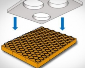
09/15/2025 | Michael Carano -- Column: Trouble in Your TankDirect metallization systems based on conductive graphite are gaining popularity throughout the world. The environmental and productivity gains achievable with this process are outstanding. Direct metallization reduces the costs of compliance, waste treatment, and legal issues related to chemical exposure. A graphite-based direct plate system has been devised to address these needs.
Closing the Loop on PCB Etching Waste
09/09/2025 | Shawn Stone, IECAs the PCB industry continues its push toward greener, more cost-efficient operations, Sigma Engineering’s Mecer System offers a comprehensive solution to two of the industry’s most persistent pain points: etchant consumption and rinse water waste. Designed as a modular, fully automated platform, the Mecer System regenerates spent copper etchants—both alkaline and acidic—and simultaneously recycles rinse water, transforming a traditionally linear chemical process into a closed-loop system.
Driving Innovation: Depth Routing Processes—Achieving Unparalleled Precision in Complex PCBs
09/08/2025 | Kurt Palmer -- Column: Driving InnovationIn PCB manufacturing, the demand for increasingly complex and miniaturized designs continually pushes the boundaries of traditional fabrication methods, including depth routing. Success in these applications demands not only on robust machinery but also sophisticated control functions. PCB manufacturers rely on advanced machine features and process methodologies to meet their precise depth routing goals. Here, I’ll explore some crucial functions that empower manufacturers to master complex depth routing challenges.
Trouble in Your Tank: Minimizing Small-via Defects for High-reliability PCBs
08/27/2025 | Michael Carano -- Column: Trouble in Your TankTo quote the comedian Stephen Wright, “If at first you don’t succeed, then skydiving is not for you.” That can be the battle cry when you find that only small-diameter vias are exhibiting voids. Why are small holes more prone to voids than larger vias when processed through electroless copper? There are several reasons.
The Government Circuit: Navigating New Trade Headwinds and New Partnerships
08/25/2025 | Chris Mitchell -- Column: The Government CircuitAs global trade winds continue to howl, the electronics manufacturing industry finds itself at a critical juncture. After months of warnings, the U.S. Government has implemented a broad array of tariff increases, with fresh duties hitting copper-based products, semiconductors, and imports from many nations. On the positive side, tentative trade agreements with Europe, China, Japan, and other nations are providing at least some clarity and counterbalance.