


 American Made Advocacy: Five Years of Educating, Advocating, and Influencing Legislation and Policy
 Defense Speak Interpreted: Understanding What the Department of Defense Is, and Isn’t
 The Right Approach: The End of an Era—DoD Proposes MIL-PRF-31032 Cancellation


Introduction
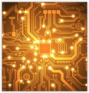
A printed circuit board is populated with a multitude of electro-mechanical components plus various active and passive devices such as transistors, capacitors, inductors and resistors, which enable the functionality and assembly of the PCB. Increasing the density of the components on the surface of a board enables greater functionality and use. A high-density (HD) design is desirable for technology high end applications, which include automotive, aerospace, space, defense, mobile phones, medical, networking, communications, and computer storage[1].
The current trend in PCB markets is lowtechnology, high-volume demand and is typically supplied by low-cost, large-scale facilities in Southeast Asia, such as China, India and Thailand. High-value, low-volume PCB markets are typically supplied by smaller-sized facilities in western regions such as North America and Europe, but also economically developed east
ern locations such as Japan, South Korea and Taiwan[2]. The UK PCB demand typically focuses on this latter market. Manufacturing developments bringing increased capability and cost savings to a factory in the UK would be highly desirable and enable increased market competitiveness. For more than four years, Merlin Circuit Technology Ltd (MCT), in Deeside, North Wales, has been working in collaboration with Heriot-Watt University (HWU) in Edinburgh, Scotland, on a UK government project funded by the Engineering and Physical Sciences Research Council (EPSRC), looking to improve HD PCB manufacturing capability through enhancements to the electrodeposition of copper using high frequency acoustic, applied within a copper plating bath [3,4,5]. This article outlines some of the key findings from this project.
To read the full version of this article which appeared in the June 2017 issue of The PCB Magazine.


