


 The Marketing Minute: Cracking the Code of Technical Marketing
 Trouble in Your Tank: Implementing Direct Metallization in Advanced Substrate Packaging


Seeing The Invisible With a Graphene-CMOS Integrated Device
July 7, 2017 | Graphene FlagshipEstimated reading time: 2 minutes
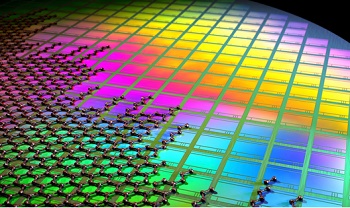
Silicon based CMOS (Complementary metal-oxide semiconductors) technology has truly shaped our world. It enables most of the electronics that we rely on today including computers, smartphones and digital cameras. However, to continue the path of progress in the electronics industry new technology must be developed and a key feature of this is the ability to integrate CMOS with other semiconductors. Now, Graphene Flagship researchers from ICFO (The Institute of Photonic Sciences in Barcelona) have shown that it is possible to integrate graphene into a CMOS integrated circuit.
In their paper published in the journal Nature Photonics they combine this graphene-CMOS device with quantum dots to create an array of photodetectors, producing a high resolution image sensor. When used as a digital camera this device is able to sense UV, visible and infrared light at the same time. This is just one example of how this device might be used, others include in microelectronics, sensor arrays and low-power photonics.
“The development of this monolithic CMOS-based image sensor represents a milestone for low-cost, high-resolution broadband and hyperspectral imaging systems” ICREA Professor at ICFO, Frank Koppens, highlights. He assures that “in general, graphene-CMOS technology will enable a vast amount of applications, that range from safety, security, low cost pocket and smartphone cameras, fire control systems, passive night vision and night surveillance cameras, automotive sensor systems, medical imaging applications, food and pharmaceutical inspection to environmental monitoring, to name a few”.
These results were enabled by the collaboration between Graphene Flagship Partner Graphenea (a Spanish graphene supplier) and ICFO, within the optoelectronics workpackage of the Graphene Flagship.
By creating a hybrid graphene and quantum dot system on a CMOS wafer using a layering and patterning approach, the Flagship team solved a complex problem with a simple solution. First the graphene is deposited, then patterned to define the pixel shape and finally a layer of PbS colloidal quantum dots is added. The photoresponse of this system is based on a photogating effect, which starts as the quantum dot layer absorbs light and transfers it as photo-generated holes or electrons to the graphene, where they circulate due to a bias voltage applied between two pixel contacts. The photo signal is then sensed by the change in conductivity of the graphene, with graphene’s high charge mobility allowing for the high sensitivity of the device.
As Stijn Goossens comments, “No complex material processing or growth processes were required to achieve this graphene-quantum dot CMOS image sensor. It proved easy and cheap to fabricate at room temperature and under ambient conditions, which signifies a considerable decrease in production costs. Even more, because of its properties, it can be easily integrated on flexible substrates as well as CMOS-type integrated circuits.”
The commercial applications of this research and the potential for imaging and sensing technology are now being explored in ICFO’s Launchpad incubator.
Professor Andrea Ferrari, Science and Technology Officer and Chair of the Management Panel of the Graphene Flagship added: "The integration of graphene with CMOS technology is a cornerstone for the future implementation of graphene in consumer electronics. This work is a key first step, clearly demonstrating the feasibility of this approach. The Flagship has put a significant investment in the system level integration of graphene, and this will increase as we move along the technology and innovation roadmap".
Share on:


Testimonial
"Our marketing partnership with I-Connect007 is already delivering. Just a day after our press release went live, we received a direct inquiry about our updated products!"
Rachael Temple - AlltematedSuggested Items
Curing and Verification in PCB Shadow Areas
09/17/2025 | Doug Katze, DymaxDesign engineers know a simple truth that often complicates electronics manufacturing: Light doesn’t go around corners. In densely populated PCBs, adhesives and coatings often fail to fully cure in shadowed regions created by tall ICs, connectors, relays, and tight housings.
Altair, Wichita State University’s NIAR Sign MoU to Accelerate Aerospace Innovation
09/16/2025 | AltairAltair, a global leader in computational intelligence, and Wichita State University’s (WSU) National Institute for Aviation Research (NIAR), one of the world’s leading aerospace research institutions, have signed a memorandum of understanding (MoU) to advance innovation across the aerospace and defense industries.
AI-Powered Wearables Transform How Consumers Interact with Everyday Technology
09/15/2025 | PR NewswireThe global demand for AI-driven, touchless wearable technologies is accelerating as consumers seek more natural, seamless and intuitive ways to interact with their devices. Traditional touch screens and voice assistants, while effective, are increasingly viewed as limiting in a world where multitasking, mobility and efficiency are key. As industries from consumer electronics to augmented reality and enterprise computing embrace the possibilities of gesture-based control, the market for neural interfaces is rapidly expanding
Hanwha Aerospace to Collaborate with BAE Systems on Advanced Anti-jamming GPS for Guided Missiles
09/15/2025 | HanwhaHanwha Aerospace has signed a contract with BAE Systems to integrate next-generation, anti-jamming Global Positioning System (GPS) technology into Hanwha Aerospace’s Deep Strike Capability precision-guided weapon system.
United Electronics Corporation Unveils Revolutionary CIMS Galaxy 30 Automated Optical Inspection System
09/11/2025 | United Electronics CorporationUnited Electronics Corporation (UEC) today announced the launch of its new groundbreaking CIMS Galaxy 30 Automated Optical Inspection (AOI) machine, setting a new industry standard for precision electronics manufacturing quality control. The Galaxy 30, developed and manufactured by CIMS, represents a significant leap forward in inspection technology, delivering exceptional speed improvements and introducing cutting-edge artificial intelligence capabilities.