


 Trouble in Your Tank: Implementing Direct Metallization in Advanced Substrate Packaging
 It’s Only Common Sense: Storytelling That Sells—Stop Pitching, Start Painting Pictures
 The Right Approach: Get Ready for ISO 9001 Version 6


Semiconductor Manufacturing: What Is Driving the Growth of the Glass Material Market?
July 14, 2017 | Yole DéveloppementEstimated reading time: 2 minutes
Used either as a permanent or as a temporary material within the semiconductor manufacturing processes, glass plays a key role in the semiconductor industry. It is today already implemented as a mature solution, in several market segments such as IR cut filter for CIS technology, microfluidics devices and some actuators and sensors.
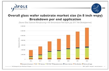
Yole Développement (Yole) confirms the growth of the glass materials market for the next five years. Therefore, the 8-inch eq glass wafer market is expected to increase at a 23% CAGR through 2022, reaching around 14M 8-inch eq wafer. Related revenue will exceed almost 594$ million by 2022, explain Yole’s analysts. Why will the glass wafer market’s revenue more than double over the next five years?
Yole’s analysts propose today a new technology & market analysis dedicated to glass materials for semiconductor manufacturing, titled Glass Substrate Manufacturing in the Semiconductor Field. This report provides detailed information regarding the current and potential applicability of glass material in the semiconductor field, as well as its processing functionalities. Analysts also review in this report major applications currently using glass material as well as potential applications that could require glass.
“Glass is making serious inroads in the semiconductor market, adopting various functionalities within IC semiconductor devices,” asserts Amandine Pizzagalli, Technology & Market Analyst, Advanced Packaging & Semiconductor Manufacturing at Yole.
Specific to semiconductors, glass material is typically developed in two formats wafer and panel, and is available in two densities, thin and thick. Moreover, glass material can be used in two different ways to fabricate a semiconductor device’s product:
- Glass-based product where the glass material is applied as a permanent material and remains in the final product.
- A non-glass-based product where the glass substrate is only applied for temporary use in the process flow and then removed after the IC device is processed.
Some IC device applications using glass material are mature, such as CIS, microfluidics, and actuators & sensors, with relatively low growth opportunity except for FO WLP packaging applications driven by glass carrier usage.
Regarding functionalities, WLCapping and permanent substrate, both fueled by the automotive and medical fields, drive the development of the glass wafer market.
The glass material market’s ascent will be due to the fast growth of glass carriers for FO WLP and actuators & sensors. On the other side, TGV interposer is still perceived as immature, but Yole is expecting an adoption rate for production by 2019 - 2020.
The glass material market for semiconductor is concentrated amongst glass material suppliers from different categories:
- Raw material manufacturers like Schott, Corning, and AGC providing raw glass material and blank wafers or sheets. These companies have limited wafer-processing capabilities.
- Glass processors and structured substrate manufacturers like PlanOptik and Tecnisco, which can pattern and structure glass wafers from the raw material provided by raw material suppliers. These companies typically purchase wafers from raw-glass material suppliers and then design/create products from the raw material.
- Structured/patterned glass wafer manufacturer mainly from MEMS & microfluidics areas, focused mainly on microfluidic and MEMS devices. This category mostly includes foundries that start from blank or pre-patterned wafers. However, contrary to a typical foundry such as Silex Microsystems, these companies create their own products.
Established glass applications such as CIS and microfluidics have led Schott to dominate the glass material market in the semiconductor field. However, emerging applications including RF devices, FO WLP technology and more… could require the use of glass material. These emerging fields represent a real business opportunities for some glass companies.
Share on:


Testimonial
"The I-Connect007 team is outstanding—kind, responsive, and a true marketing partner. Their design team created fresh, eye-catching ads, and their editorial support polished our content to let our brand shine. Thank you all! "
Sweeney Ng - CEE PCBSuggested Items
Curing and Verification in PCB Shadow Areas
09/17/2025 | Doug Katze, DymaxDesign engineers know a simple truth that often complicates electronics manufacturing: Light doesn’t go around corners. In densely populated PCBs, adhesives and coatings often fail to fully cure in shadowed regions created by tall ICs, connectors, relays, and tight housings.
Altair, Wichita State University’s NIAR Sign MoU to Accelerate Aerospace Innovation
09/16/2025 | AltairAltair, a global leader in computational intelligence, and Wichita State University’s (WSU) National Institute for Aviation Research (NIAR), one of the world’s leading aerospace research institutions, have signed a memorandum of understanding (MoU) to advance innovation across the aerospace and defense industries.
AI-Powered Wearables Transform How Consumers Interact with Everyday Technology
09/15/2025 | PR NewswireThe global demand for AI-driven, touchless wearable technologies is accelerating as consumers seek more natural, seamless and intuitive ways to interact with their devices. Traditional touch screens and voice assistants, while effective, are increasingly viewed as limiting in a world where multitasking, mobility and efficiency are key. As industries from consumer electronics to augmented reality and enterprise computing embrace the possibilities of gesture-based control, the market for neural interfaces is rapidly expanding
Hanwha Aerospace to Collaborate with BAE Systems on Advanced Anti-jamming GPS for Guided Missiles
09/15/2025 | HanwhaHanwha Aerospace has signed a contract with BAE Systems to integrate next-generation, anti-jamming Global Positioning System (GPS) technology into Hanwha Aerospace’s Deep Strike Capability precision-guided weapon system.
United Electronics Corporation Unveils Revolutionary CIMS Galaxy 30 Automated Optical Inspection System
09/11/2025 | United Electronics CorporationUnited Electronics Corporation (UEC) today announced the launch of its new groundbreaking CIMS Galaxy 30 Automated Optical Inspection (AOI) machine, setting a new industry standard for precision electronics manufacturing quality control. The Galaxy 30, developed and manufactured by CIMS, represents a significant leap forward in inspection technology, delivering exceptional speed improvements and introducing cutting-edge artificial intelligence capabilities.