


 Trouble in Your Tank: Implementing Direct Metallization in Advanced Substrate Packaging
 It’s Only Common Sense: Storytelling That Sells—Stop Pitching, Start Painting Pictures
 The Right Approach: Get Ready for ISO 9001 Version 6


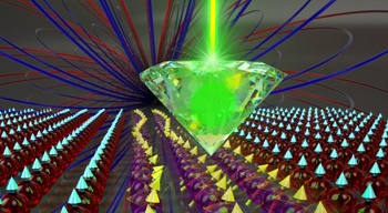
Researchers Develop Technique to Control and Measure Electron Spin Voltage
July 14, 2017 | Harvard UniversityEstimated reading time: 3 minutes
Information technologies of the future will likely use electron spin — rather than electron charge — to carry information. But first, scientists need to better understand how to control spin and learn to build the spin equivalent of electronic components, from spin transistors, to spin gates and circuits.
Now, researchers from Harvard University have developed a technique to control and measure spin voltage, known as spin chemical potential. The technique, which uses atomic-sized defects in diamonds to measure chemical potential, is essentially a nanoscale spin multimeter that allows measurements in chip-scale devices.
“There is growing interest in insulating materials that can conduct spin,” said Amir Yacoby, Professor of Physics in the Department of Physics and of Applied Physics at Harvard John A. Paulson School of Engineering and Applied Sciences and senior author of the paper. “Our work develops a new way to look at these spins in materials such as magnets.”
In conducting materials, electrons can carry information by moving from point A to point B. This is an electric current. Spin, on the other hand, can propagate through insulating materials in waves, each electron standing still and communicating spin to its coupled neighbor, like a quantum game of telephone.
To drive these waves from point A to point B, the researchers needed to develop a technique to increase the spin chemical potential — spin voltage — at a local level.
“If you have a high chemical potential at location A and a low chemical potential at location B, spin waves start diffusing from A to B,” said Chunhui Du, a postdoctoral fellow at the Department of Physics and co-first author of the paper. “This is a very important concept in spintronics, because if you are able to control spin-wave transport, then you can use these spin waves instead of electrical current as carriers of information.”
The researchers used two spin-wave injection methods: in the first, they applied fast-oscillating, microwave magnetic fields to excite spin waves. In the second, they converted an electrical current into spin waves using a platinum metal strip located at one end of the magnet.
“What’s remarkable is that this material is an insulator; it doesn’t conduct any current and still you can send information in the form of spin waves through it,” said Toeno Van der Sar, a postdoctoral fellow at the Department of Physics and co-first author of the paper. “Spin waves are so promising because they can travel for a long time without decaying, and there is barely any heat produced because you don’t have moving electrons.”
These defects — in which one carbon atom in a diamond is replaced with a nitrogen atom and a neighboring atom is removed — can be used to detect minute magnetic fields.
Tweet This
Once the team injected spin waves into the material, the next step was to figure out how to measure information about those waves. The researchers turned to nitrogen-vacancy (NV) defects in diamonds. These defects — in which one carbon atom in a diamond is replaced with a nitrogen atom and a neighboring atom is removed — can be used to detect minute magnetic fields.
The researchers fabricated tiny rods of diamond containing NV centers and placed them nanometers above the sample. As the spin waves move through the material, they generate a magnetic field, which is picked up by the NV center.
Based on NV-center measurements, researchers can now figure out the spin chemical potential, the number of spin waves, how they are moving through the material and other important insights.
“The nice thing about this technique is that it’s very local,” said Van der Sar. “You can do these measurements just a few nanometers above the sample, which means that you can spatially study the chemical potential in a chip-scale spin-wave device, for let’s say a spin-wave computer. This is not possible with some of the other state–of-the-art techniques.”
This system could also offer a glimpse into more exotic physics such as the spin-wave Hall effect, or show that spin-wave transport is hydrodynamic.
“The principle we use to control and measure the spin chemical potential is quite general. It opens ways to study more exotic spin phenomena in novel materials and aids the development of new spintronic devices,” said Du.
This research was supported in part by the Gordon and Betty Moore Foundation’s Emergent Phenomena in Quantum Systems (EPiQS) Initiative, the Multidisciplinary University Research Initiative (MURI) Quibit Enabled Imaging, Sensing, and Metrology (QuISM) project and the Army Research Office.
Original by: Leah Burrows
Share on:


Testimonial
"In a year when every marketing dollar mattered, I chose to keep I-Connect007 in our 2025 plan. Their commitment to high-quality, insightful content aligns with Koh Young’s values and helps readers navigate a changing industry. "
Brent Fischthal - Koh YoungSuggested Items
Curing and Verification in PCB Shadow Areas
09/17/2025 | Doug Katze, DymaxDesign engineers know a simple truth that often complicates electronics manufacturing: Light doesn’t go around corners. In densely populated PCBs, adhesives and coatings often fail to fully cure in shadowed regions created by tall ICs, connectors, relays, and tight housings.
September 2025 PCB007 Magazine: The Future of Advanced Materials
09/16/2025 | I-Connect007 Editorial TeamMoore’s Law is no more, and the advanced material solutions being developed to grapple with this reality are surprising, stunning, and perhaps a bit daunting. Buckle up for a dive into advanced materials and a glimpse into the next chapters of electronics manufacturing.
I-Connect007 Launches Advanced Electronics Packaging Digest
09/15/2025 | I-Connect007I-Connect007 is pleased to announce the launch of Advanced Electronics Packaging Digest (AEPD), a new monthly digital newsletter dedicated to one of the most critical and rapidly evolving areas of electronics manufacturing: advanced packaging at the interconnect level.
Panasonic Industry will Double the Production Capacity of MEGTRON Multi-layer Circuit Board Materials Over the Next Five Years
09/15/2025 | Panasonic Industry Co., Ltd.Panasonic Industry Co., Ltd., a Panasonic Group company, announced plans for a major expansion of its global production capacity for MEGTRON multi-layer circuit board materials today. The company plans to double its production over the next five years to meet growing demand in the AI server and ICT infrastructure markets.
Trouble in Your Tank: Implementing Direct Metallization in Advanced Substrate Packaging
09/15/2025 | Michael Carano -- Column: Trouble in Your TankDirect metallization systems based on conductive graphite are gaining popularity throughout the world. The environmental and productivity gains achievable with this process are outstanding. Direct metallization reduces the costs of compliance, waste treatment, and legal issues related to chemical exposure. A graphite-based direct plate system has been devised to address these needs.