


 Trouble in Your Tank: Implementing Direct Metallization in Advanced Substrate Packaging
 It’s Only Common Sense: Storytelling That Sells—Stop Pitching, Start Painting Pictures
 The Right Approach: Get Ready for ISO 9001 Version 6


Computer Chip Technology Repurposed for Making Reflective Nanostructures
July 18, 2017 | CaltechEstimated reading time: 2 minutes
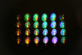
A team of engineers at Caltech has discovered how to use computer-chip manufacturing technologies to create the kind of reflective materials that make safety vests, running shoes, and road signs appear shiny in the dark.
Those materials owe their shininess to retroreflection, a property that allows them to bounce light directly back to its source from a wide variety of angles. In contrast, a basic flat mirror will not bounce light back to its source if that light is coming from any angle other than straight on.
Retroreflectors' ability to return light to where it came from makes them useful for highlighting objects that need to be seen in dark conditions. For example, if light from a car's headlights shines on the safety vest of a construction worker down the road, the vest's retroreflective strips will bounce that light straight back to the car and into the driver's eyes, making the vest appear to glow.
Retroreflectors have also been used in surveyors' equipment, communications with satellites, and even in experiments to measure the distance of the moon from Earth.
Typically, retroreflectors consist of tiny glass spheres embedded in the surface of reflective paint or in small mirrors shaped like the inner corner of a cube.
The new technology—which was developed by a team led by Caltech's Andrei Faraon, assistant professor of applied physics and materials science in the Division of Engineering and Applied Science—uses surfaces covered by a metamaterial consisting of millions of silicon pillars, each only a few hundred nanometers tall. By adjusting the size of the pillars and the spacing between them, Faraon can manipulate how the surface reflects, refracts, or transmits light. He has already shown that these materials can be tweaked to create flat lenses for focusing light or to create prism-like surfaces that spread the light out into its spectrum. Now, he's discovered that he can build a retroreflector by stacking two layers of the metamaterials atop one another.
In this kind of retroreflector, light first passes through a transparent metamaterial layer (metasurface) and is focused by its tiny pillars onto a single spot on a reflective metamaterial layer. The reflective layer then bounces the light back to the transparent layer, which transmits the light back to its source.
"By placing multiple metasurfaces on top of each other, it is possible to control the flow of light in such a way that was not possible before," Faraon says. "The functionality of a retroreflector cannot be achieved by using a single metasurface."
Since Faraon's metamaterials are created using computer-chip manufacturing technologies, it would be possible to easily integrate them into chips used in optoelectronic devices—electronics that use and control light, he says.
"This could have applications in communicating with remote sensors, drones, satellites, etc.," he adds.
Faraon's research appears in a paper in the June 19, 2017, edition of Nature Photonics; the paper is titled "Planar metasurface retroreflector." Other coauthors are Amir Arbabi, assistant professor of computer and electrical engineering at the University of Massachusetts Amherst; and Caltech electrical engineering graduate students Ehsan Arbabi, Yu Horie, and Seyedeh Mahsa Kamali.
The project was supported by the Jet Propulsion Laboratory, DARPA, Northrop Grumman, the Japan Student Services Organization, and the U.S. Department of Energy.
Share on:


Testimonial
"The I-Connect007 team is outstanding—kind, responsive, and a true marketing partner. Their design team created fresh, eye-catching ads, and their editorial support polished our content to let our brand shine. Thank you all! "
Sweeney Ng - CEE PCBSuggested Items
Curing and Verification in PCB Shadow Areas
09/17/2025 | Doug Katze, DymaxDesign engineers know a simple truth that often complicates electronics manufacturing: Light doesn’t go around corners. In densely populated PCBs, adhesives and coatings often fail to fully cure in shadowed regions created by tall ICs, connectors, relays, and tight housings.
September 2025 PCB007 Magazine: The Future of Advanced Materials
09/16/2025 | I-Connect007 Editorial TeamMoore’s Law is no more, and the advanced material solutions being developed to grapple with this reality are surprising, stunning, and perhaps a bit daunting. Buckle up for a dive into advanced materials and a glimpse into the next chapters of electronics manufacturing.
I-Connect007 Launches Advanced Electronics Packaging Digest
09/15/2025 | I-Connect007I-Connect007 is pleased to announce the launch of Advanced Electronics Packaging Digest (AEPD), a new monthly digital newsletter dedicated to one of the most critical and rapidly evolving areas of electronics manufacturing: advanced packaging at the interconnect level.
Panasonic Industry will Double the Production Capacity of MEGTRON Multi-layer Circuit Board Materials Over the Next Five Years
09/15/2025 | Panasonic Industry Co., Ltd.Panasonic Industry Co., Ltd., a Panasonic Group company, announced plans for a major expansion of its global production capacity for MEGTRON multi-layer circuit board materials today. The company plans to double its production over the next five years to meet growing demand in the AI server and ICT infrastructure markets.
Trouble in Your Tank: Implementing Direct Metallization in Advanced Substrate Packaging
09/15/2025 | Michael Carano -- Column: Trouble in Your TankDirect metallization systems based on conductive graphite are gaining popularity throughout the world. The environmental and productivity gains achievable with this process are outstanding. Direct metallization reduces the costs of compliance, waste treatment, and legal issues related to chemical exposure. A graphite-based direct plate system has been devised to address these needs.