


 Trouble in Your Tank: Implementing Direct Metallization in Advanced Substrate Packaging
 It’s Only Common Sense: Storytelling That Sells—Stop Pitching, Start Painting Pictures
 The Right Approach: Get Ready for ISO 9001 Version 6


Nanoparticles Could Spur Better LEDs, Invisibility Cloaks
July 20, 2017 | University of MichiganEstimated reading time: 4 minutes
In an advance that could boost the efficiency of LED lighting by 50% and even pave the way for invisibility cloaking devices, a team of University of Michigan researchers has developed a new technique that peppers metallic nanoparticles into semiconductors.
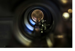
The inside of the main concourse of the molecular beam epitaxy apparatus, which University of Michigan engineering researchers used to make the advanced nanoparticle-infused gallium nitride semiconductors. The semiconductors could boost LED efficiency by up to 50%, and even lead to invisibility cloaking devices. Image credit: Joseph Xu, Michigan Engineering
It's the first technique that can inexpensively grow metal nanoparticles both on and below the surface of semiconductors. The process adds virtually no cost during manufacturing and its improved efficiency could allow manufacturers to use fewer semiconductors in finished products, making them less expensive.
The metal nanoparticles can increase the efficiency of LEDs in several ways. They can act as tiny antennas that alter and redirect the electricity running through the semiconductor, turning more of it into light. They can also help reflect light out of the device, preventing it from being trapped inside and wasted.
The main growth chamber of the molecular epitaxy beam apparatus used to make the nanoparticle-infused gallium nitride semiconductors. The semiconductors could boost LED efficiency by up to 50 percent, and even lead to invisibility cloaking devices. Image credit: Joseph Xu, Michigan Engineering
The process can be used with the gallium nitride that's used in LED lighting and can also boost efficiency in other semiconductor products, including solar cells. It's detailed in a study published in the Journal of Applied Physics.
"This is a seamless addition to the manufacturing process, and that's what makes it so exciting," said Rachel Goldman, U-M professor of materials science and engineering, and physics. "The ability to make 3-D structures with these nanoparticles throughout is going to open a lot of possibilities."
The key innovation
The idea of adding nanoparticles to increase LED efficiency is not new. But previous efforts to incorporate them have been impractical for large-scale manufacturing. They focused on pricey metals like silver, gold and platinum. In addition, the size and spacing of the particles must be very precise; this required additional and expensive manufacturing steps. Furthermore, there was no cost-effective way to incorporate particles below the surface.
Former materials science PhD student Sunyeol Jun prepares the molecular beam epitaxy apparatus that’s used to make the nanoparticle-infused gallium nitride semiconductors. The semiconductors could boost LED efficiency by up to 50%, and even lead to invisibility cloaking devices. Image credit: Joseph Xu, Michigan Engineering
Goldman's team discovered a simpler way that integrates easily with the molecular beam epitaxy process used to make semiconductors. Molecular beam epitaxy sprays multiple layers of metallic elements onto a wafer. This creates exactly the right conductive properties for a given purpose.
The U-M researchers applied an ion beam between these layers—a step that pushes metal out of the semiconductor wafer and onto the surface. The metal forms nanoscale particles that serve the same purpose as the pricey gold and platinum flecks in earlier research. Their size and placement can be precisely controlled by varying the angle and intensity of the ion beam. And applying the ion beam over and over between each layer creates a semiconductor with the nanoparticles interspersed throughout.
"If you carefully tailor the size and spacing of nanoparticles and how deeply they're embedded, you can find a sweet spot that enhances light emissions," said Myungkoo Kang, a former graduate student in Goldman's lab and first author on the study. "This process gives us a much simpler and less expensive way to do that."
A microscopy photo showing an array of precisely placed metallic nanoparticles on the surface of a gallium arsenide semiconductor. Image courtesy: Rachel S. Goldman, Michigan Engineering
Researchers have known for years that metallic particles can collect on the surface of semiconductors during manufacturing. But they were always considered a nuisance, something that happened when the mix of elements was incorrect or the timing was off.
"From the very early days of semiconductor manufacturing, the goal was always to spray a smooth layer of elements onto the surface. If the elements formed particles instead, it was considered a mistake," Goldman said. "But we realized that those 'mistakes' are very similar to the particles that manufacturers have been trying so hard to incorporate into LEDs. So, we figured out a way to make lemonade out of lemons."
Toward invisibility cloaks
Because the technique allows precise control over the nanoparticle distribution, the researchers say it may one day be useful for cloaks that render objects partially invisible by inducing a phenomenon known as "reverse refraction."
Reverse refraction bends light waves backwards in a way that doesn't occur in nature, potentially directing them around an object or away from the eye. The researchers believe that by carefully sizing and spacing an array of nanoparticles, they may be able to induce and control reverse refraction in specific wavelengths of light.
"For invisibility cloaking, we need to both transmit and manipulate light in very precise ways, and that's very difficult today," Goldman said. "We believe that this process could give us the level of control we need to make it work."
The team is now working to adapt the ion beam process to the specific materials used in LEDs—they estimate that the higher-efficiency lighting devices could be ready for market within the next five years, with invisibility cloaking and other applications coming further in the future.
The study is titled "Formation of embedded plasmonic Ga nanoparticle arrays and their influence on GaAs photoluminescence." The research was supported by the National Science Foundation through the Materials Research Science and Engineering Center at U-M.
Share on:


Testimonial
"Our marketing partnership with I-Connect007 is already delivering. Just a day after our press release went live, we received a direct inquiry about our updated products!"
Rachael Temple - AlltematedSuggested Items
Alternative Manufacturing, Inc. (AMI) Announces Commitment to Excellence in Industrial, Defense, Aerospace, Renewables, and Robotics Markets
09/16/2025 | Alternative Manufacturing, Inc.Alternative Manufacturing, Inc. (AMI), a 100% employee-owned contract manufacturer, proudly reaffirms its leadership in the electronics manufacturing services (EMS) industry with a continued commitment to delivering high-quality PCBAs and box builds across the industrial, defense, aerospace, renewable energy, and robotics markets.
Sustainability and Selective Soldering
09/15/2025 | Dr. Samuel J. McMaster, Pillarhouse InternationalSustainability is more than just a buzzword for the electronics industry; it’s a key goal for all manufacturing processes. This is more than a box-ticking exercise or simply doing a small part for environmentally friendly processes. Moving toward sustainable solutions drives innovation and operational efficiency.
Trouble in Your Tank: Implementing Direct Metallization in Advanced Substrate Packaging
09/15/2025 | Michael Carano -- Column: Trouble in Your TankDirect metallization systems based on conductive graphite are gaining popularity throughout the world. The environmental and productivity gains achievable with this process are outstanding. Direct metallization reduces the costs of compliance, waste treatment, and legal issues related to chemical exposure. A graphite-based direct plate system has been devised to address these needs.
EV Group Achieves Breakthrough in Hybrid Bonding Overlay Control for Chiplet Integration
09/12/2025 | EV GroupEV Group (EVG), a leading provider of innovative process solutions and expertise serving leading-edge and future semiconductor designs and chip integration schemes, today unveiled the EVG®40 D2W—the first dedicated die-to-wafer overlay metrology platform to deliver 100 percent die overlay measurement on 300-mm wafers at high precision and speeds needed for production environments. With up to 15X higher throughput than EVG’s industry benchmark EVG®40 NT2 system designed for hybrid wafer bonding metrology, the new EVG40 D2W enables chipmakers to verify die placement accuracy and take rapid corrective action, improving process control and yield in high-volume manufacturing (HVM).
Integrating Uniplate PLBCu6 With the Digital Factory Suite
09/12/2025 | Giovanni Obino and Andreas Schatz, MKS' AtotechPrinted circuit board manufacturing is rapidly changing, driven by miniaturization, stringent reliability requirements, and growing pressure for sustainable production. Meeting these challenges requires more than incremental improvements; it demands a combination of precise equipment and real-time process intelligence. The pairing of Uniplate® PLBCu6 with the Digital Factory Suite (DFS) demonstrates how hardware and software can work together to create more responsive, resource-efficient manufacturing.