


 Trouble in Your Tank: Implementing Direct Metallization in Advanced Substrate Packaging
 It’s Only Common Sense: Storytelling That Sells—Stop Pitching, Start Painting Pictures
 The Right Approach: Get Ready for ISO 9001 Version 6


New Method Promises Easier Nanoscale Manufacturing
July 28, 2017 | University of ChicagoEstimated reading time: 2 minutes
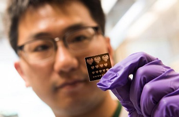
Scientists at the University of Chicago and Argonne National Laboratory have discovered a new way to precisely pattern nanomaterials that could open a new path to the next generation of everyday electronic devices.
The new research, published in Science, is expected to make such materials easily available for eventual use in everything from LED displays to cellular phones to photodetectors and solar cells. Though nanomaterials are promising for future devices, ways to build them into complex structures have been limited and small-scale.
“This is a step needed to move quantum dots and many other nanomaterials from proof-of-concept experiments to real technology we can use,” said co-author Dmitri Talapin, professor of chemistry at UChicago and a scientist with the Center for Nanoscale Materials at Argonne. “It really expands our horizons.”
Examples of optically patterned inorganic materials. The top row demonstrates negative patterning, and the bottom row demonstrates positive patterning. Courtesy ofDmitri Talapin and Yuanyuan Wang / Illustration by UChicago Creative
The foundation of modern computing is a tiny switch called the transistor, made billions at a time by a technique called photolithography. This process, which has made smartphones cheap and ubiquitous, carves a stencil out of a layer of organic polymer by laying down a patterned “mask” and illuminating it with ultraviolet light. After the new material is deposited on top, the polymer stencil is lifted off to reveal the pattern. Several rounds of such patterning build a miniature transistor onto the material.
But the method has its limitations. Only a few materials can be patterned this way; it was originally developed for silicon, and as silicon’s half-century reign over electronics reaches its end, scientists are looking ahead to the next materials.
One such avenue of interest is nanomaterials—tiny crystals of metals or semiconductors. At this scale, they can have unique and useful properties, but manufacturing devices out of them has been difficult.
The new technique, called DOLFIN, makes different nanomaterials directly into “ink” in a process that bypasses the need to lay down a polymer stencil. Talapin and his team carefully designed chemical coatings for individual particles. These coatings react with light, so if you shine light through a patterned mask, the light will transfer the pattern directly into the layer of nanoparticles below—wiring them into useful devices.
“We found the quality of the patterns was comparable to those made with state-of-the-art techniques,” said lead author Yuanyuan Wang, postdoctoral researcher at UChicago. “It can be used with a wide range of materials, including semiconductors, metals, oxides or magnetic materials—all commonly used in electronics manufacturing.”
Share on:


Testimonial
"In a year when every marketing dollar mattered, I chose to keep I-Connect007 in our 2025 plan. Their commitment to high-quality, insightful content aligns with Koh Young’s values and helps readers navigate a changing industry. "
Brent Fischthal - Koh YoungSuggested Items
Curing and Verification in PCB Shadow Areas
09/17/2025 | Doug Katze, DymaxDesign engineers know a simple truth that often complicates electronics manufacturing: Light doesn’t go around corners. In densely populated PCBs, adhesives and coatings often fail to fully cure in shadowed regions created by tall ICs, connectors, relays, and tight housings.
September 2025 PCB007 Magazine: The Future of Advanced Materials
09/16/2025 | I-Connect007 Editorial TeamMoore’s Law is no more, and the advanced material solutions being developed to grapple with this reality are surprising, stunning, and perhaps a bit daunting. Buckle up for a dive into advanced materials and a glimpse into the next chapters of electronics manufacturing.
I-Connect007 Launches Advanced Electronics Packaging Digest
09/15/2025 | I-Connect007I-Connect007 is pleased to announce the launch of Advanced Electronics Packaging Digest (AEPD), a new monthly digital newsletter dedicated to one of the most critical and rapidly evolving areas of electronics manufacturing: advanced packaging at the interconnect level.
Panasonic Industry will Double the Production Capacity of MEGTRON Multi-layer Circuit Board Materials Over the Next Five Years
09/15/2025 | Panasonic Industry Co., Ltd.Panasonic Industry Co., Ltd., a Panasonic Group company, announced plans for a major expansion of its global production capacity for MEGTRON multi-layer circuit board materials today. The company plans to double its production over the next five years to meet growing demand in the AI server and ICT infrastructure markets.
Trouble in Your Tank: Implementing Direct Metallization in Advanced Substrate Packaging
09/15/2025 | Michael Carano -- Column: Trouble in Your TankDirect metallization systems based on conductive graphite are gaining popularity throughout the world. The environmental and productivity gains achievable with this process are outstanding. Direct metallization reduces the costs of compliance, waste treatment, and legal issues related to chemical exposure. A graphite-based direct plate system has been devised to address these needs.