


 Trouble in Your Tank: Implementing Direct Metallization in Advanced Substrate Packaging
 It’s Only Common Sense: Storytelling That Sells—Stop Pitching, Start Painting Pictures
 The Right Approach: Get Ready for ISO 9001 Version 6


Taking Technology to the Next Level
July 28, 2017 | CUDOSEstimated reading time: 3 minutes
Physicists from the ARC Centre of Excellence for Ultrahigh bandwidth Devices for Optical Systems (CUDOS) developed a new hybrid integrated platform that promises to be a more advanced alternative to conventional integrated circuits that are currently manufactured by the semiconductor industry. The researchers demonstrated that their approach is mass manufacturable, making it possible to integrate the platform into everyday electronic equipment like smartphones and computers. For the end user this technical advance means that it may lead to faster internet on their next-generation electronic devices.
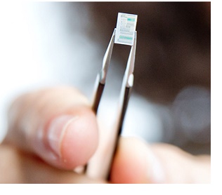
The new device is smaller than a thumbnail with a size of 0.1 x 4mm, and could be integrated into everyday electronic devices like smartphones.
Integrated circuits, so called ‘chips’, are used in everyday electronic equipment like mobile phones and computers. It is a set of electronic circuits on one small flat piece of semiconductor material, normally silicon. But this material has some limitations when it comes to processing data. To overcome these limitations and improve data processing, researchers are developing optical circuits made of chalcogenide glass. This special type of glass is used for ultrafast telecommunication networks, transferring information at the speed of light. Integrating these glass optical circuits into silicon chips could lead to a more advanced communications system, processing data a hundred times faster. Can these two materials be combined?
The answer is yes! In a collaboration with physicists in the University of Sydney’s Australian Institute for Nanoscale Science and Technology (AINST), the Australian National University (ANU) and RMIT University, the CUDOS research group around PhD candidate Blair Morrison and senior researcher Dr Alvaro Casas Bedoya created compact, mass manufacturable optical circuits with enhanced functionalities by combining nonlinear glasses with silicon-based material.
“In the last few years the group at the University of Sydney has repeatedly demonstrated exciting functionalities, such as broadband microwave devices that can enhance radar, using these novel chalcogenide glasses,” Blair Morrison said from the University of Sydney CUDOS node.
“Now we have shown it is possible to combine this material with the current industry standard platform for photonic integration, silicon,” he said.
“We integrated a novel nonlinear glass into an industrially scalable CMOS compatible platform. We maintained the key advantages of both the silicon and the glass, and made a functional and efficient ultra-compact optical circuit,” said Dr Alvaro Casas Bedoya who is the lead photonics nanofabrication manager for CUDOS.
“A wealth of new opportunities will be created, and this takes us one step closer to moving our research from the lab into industrial applications,” said Blair Morrison.
CUDOS Director and ARC Laureate Fellow Professor Benjamin Eggleton from the University of Sydney said this new approach will one day allow the industry to miniaturise the photonics functionalities from devices that are the size of a laptop to the size of a smartphone and even smaller, allowing for deployment in real world applications.
“This is exciting, because this is a platform which is more compatible with existing semiconductor manufacturing and will allow us to integrate multiple functionalities on a single silicon chip, with active and passive components, such as detectors and modulators, required for advanced applications,” said Professor Eggleton who supervised the project.
The multi-university research team went through the whole manufacturing process: The fabrication of these devices uses silicon wafers from a semiconductor foundry in Belgium, a dedicated facility in ANU’s Laser Physics Centre for the glass deposition, lithography in the RMIT University’s School of Engineering and are then characterised and tested in the University of Sydney’s AINST.
To showcase the potential of the new approach, the CUDOS researchers further demonstrated a compact novel laser based on the light-sound interactions, the first time in an integrated optical circuit.
“The breakthrough here is this realisation that we can actually interface, we can integrate that glass onto silicon and we can interface from silicon to the glass very efficiently – we can harness the best of both worlds,” Professor Eggleton said.
Professor Susan Pond, the Director of AINST, emphasized that this project is one of AINST flagship activities that deals with harnessing interactions between photons and phonon at the nanoscale. This work links fundamental research in light matter interactions at the nanoscale with an end user perspective and strong coupling to industry.
Share on:


Testimonial
"We’re proud to call I-Connect007 a trusted partner. Their innovative approach and industry insight made our podcast collaboration a success by connecting us with the right audience and delivering real results."
Julia McCaffrey - NCAB GroupSuggested Items
TTCI and The Training Connection Strengthen Electronics Manufacturing with Test Services and Training at PCB West 2025
09/16/2025 | The Test Connection Inc.The Test Connection Inc. (TTCI), a trusted provider of electronic test and manufacturing solutions, and The Training Connection LLC (TTC-LLC) will exhibit at PCB West 2025, taking place Wednesday, October 1, 2025, at the Santa Clara Convention Center in California. Visitors are invited to Booth 113 to explore the companies’ complementary expertise in test engineering services and workforce development for the electronics industry.
TTM Technologies to Exhibit at the Electronica India 2025 Exhibition in Bengaluru, India
09/16/2025 | Globe NewswireTTM Technologies, Inc., a leading global manufacturer of technology solutions, including mission systems, radio frequency (RF) components, RF microwave/microelectronic assemblies, and quick-turn and technologically advanced printed circuit boards (PCBs), will exhibit at the Electronica India 2025 trade fair, at Hall 3, booth #H41, from September 17-19, 2025, at the Bangalore International Exhibition Centre, Bengaluru, India.
Beyond the Board: What Companies Need to Know Before Entering the MilAero PCB Market
09/16/2025 | Jesse Vaughan -- Column: Beyond the BoardThe MilAero electronics supply chain offers opportunities for manufacturers that are both prestigious and strategically important. Serving prime contractors and Tier-1 suppliers can mean long-term program stability and the satisfaction of contributing to national security. At the same time, this sector is unlike commercial electronics in almost every respect. Success requires more than technical capabilities, it requires patience, preparation, attention to detail, and a clear understanding of how the business model differs.
India’s Aerospace and Defence Engineered for Power, Driven by Electronics
09/16/2025 | Gaurab Majumdar, Global Electronics AssociationWith a defence budget of $82.05 billion (2025–26) and a massive $223 billion earmarked for aerospace and defence spending over the next decade, India is rapidly positioning itself as a major player in the global defence and aerospace market.
I-Connect007 Launches Advanced Electronics Packaging Digest
09/15/2025 | I-Connect007I-Connect007 is pleased to announce the launch of Advanced Electronics Packaging Digest (AEPD), a new monthly digital newsletter dedicated to one of the most critical and rapidly evolving areas of electronics manufacturing: advanced packaging at the interconnect level.