


 Trouble in Your Tank: Implementing Direct Metallization in Advanced Substrate Packaging
 It’s Only Common Sense: Storytelling That Sells—Stop Pitching, Start Painting Pictures
 The Right Approach: Get Ready for ISO 9001 Version 6


Scientists Discover New Magnet with Nearly Massless Charge Carriers
July 31, 2017 | LSUEstimated reading time: 2 minutes
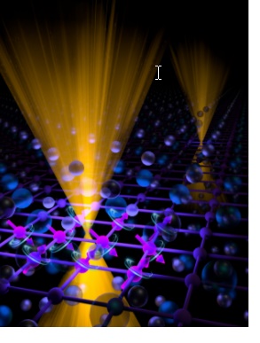
Advances in modern electronics has demanded the requisite hardware, transistors, to be smaller in each new iteration. Recent progress in nanotechnology has reduced the size of silicon transistors down to the order of 10 nanometers. However, for such small transistors, other physical effects set in, which limit their functionality. For example, the power consumption and heat production in these devices is creating significant problems for device design. Therefore, novel quantum materials and device concepts are required to develop a new generation of energy-saving information technology. The recent discoveries of topological materials — a new class of relativistic quantum materials — hold great promise for use in energy saving electronics.
Researchers in the Louisiana Consortium for Neutron Scattering, or LaCNS, led by LSU Department of Physics & Astronomy Chair and Professor John F. DiTusa and Tulane University Professor Zhiqiang Mao, with collaborators at Oak Ridge National Lab, the National High Magnetic Field Laboratory, Florida State University, and the University of New Orleans, recently reported the first observation of this topological behavior in a magnet, Sr1-yMn1-zSb2 (y, z < 0.1). These results were published this week in Nature Materials (doi:10.1038/nmat4953).
“This first observation is a significant milestone in the advancement of novel quantum materials and this discovery opens the opportunity to explore its consequences. The nearly massless behavior of the charge carriers offers possibilities for novel device concepts taking advantage of the extremely low power dissipation,” DiTusa said.
The phrase “topological materials” refers to materials where the current carrying electrons act as if they have no mass similar to the properties of photons, the particles that make up light. Amazingly, these electronic states are robust and immune to defects and disorder because they are protected from scattering by symmetry. This symmetry protection results in exceedingly high charge carrier mobility, creating little to no resistance to current flow. The result is expected to be a substantial reduction in heat production and energy saving efficiencies in electronic devices.
This new magnet displays electronic charge carriers that have almost no mass. The magnetism brings with it an important symmetry breaking property – time reversal symmetry, or TRS, breaking where the ability to run time backward would no longer return the system back to its starting conditions. The combination of relativistic electron behavior, which is the cause of much reduced charge carrier mass, and TRS breaking has been predicted to cause even more unusual behavior, the much sought after magnetic Weyl semimetal phase. The material discovered by this collaboration is thought to be an excellent one to investigate for evidence of the Weyl phase and to uncover its consequences.
Share on:


Testimonial
"In a year when every marketing dollar mattered, I chose to keep I-Connect007 in our 2025 plan. Their commitment to high-quality, insightful content aligns with Koh Young’s values and helps readers navigate a changing industry. "
Brent Fischthal - Koh YoungSuggested Items
Curing and Verification in PCB Shadow Areas
09/17/2025 | Doug Katze, DymaxDesign engineers know a simple truth that often complicates electronics manufacturing: Light doesn’t go around corners. In densely populated PCBs, adhesives and coatings often fail to fully cure in shadowed regions created by tall ICs, connectors, relays, and tight housings.
September 2025 PCB007 Magazine: The Future of Advanced Materials
09/16/2025 | I-Connect007 Editorial TeamMoore’s Law is no more, and the advanced material solutions being developed to grapple with this reality are surprising, stunning, and perhaps a bit daunting. Buckle up for a dive into advanced materials and a glimpse into the next chapters of electronics manufacturing.
I-Connect007 Launches Advanced Electronics Packaging Digest
09/15/2025 | I-Connect007I-Connect007 is pleased to announce the launch of Advanced Electronics Packaging Digest (AEPD), a new monthly digital newsletter dedicated to one of the most critical and rapidly evolving areas of electronics manufacturing: advanced packaging at the interconnect level.
Panasonic Industry will Double the Production Capacity of MEGTRON Multi-layer Circuit Board Materials Over the Next Five Years
09/15/2025 | Panasonic Industry Co., Ltd.Panasonic Industry Co., Ltd., a Panasonic Group company, announced plans for a major expansion of its global production capacity for MEGTRON multi-layer circuit board materials today. The company plans to double its production over the next five years to meet growing demand in the AI server and ICT infrastructure markets.
Trouble in Your Tank: Implementing Direct Metallization in Advanced Substrate Packaging
09/15/2025 | Michael Carano -- Column: Trouble in Your TankDirect metallization systems based on conductive graphite are gaining popularity throughout the world. The environmental and productivity gains achievable with this process are outstanding. Direct metallization reduces the costs of compliance, waste treatment, and legal issues related to chemical exposure. A graphite-based direct plate system has been devised to address these needs.