


 Trouble in Your Tank: Implementing Direct Metallization in Advanced Substrate Packaging
 It’s Only Common Sense: Storytelling That Sells—Stop Pitching, Start Painting Pictures
 The Right Approach: Get Ready for ISO 9001 Version 6


A Semiconductor That Can Beat the Heat
August 1, 2017 | Berkeley LabEstimated reading time: 5 minutes
A newly discovered collective rattling effect in a type of crystalline semiconductor blocks most heat transfer while preserving high electrical conductivity – a rare pairing that scientists say could reduce heat buildup in electronic devices and turbine engines, among other possible applications.
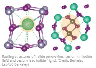
A team led by scientists at the Department of Energy’s Lawrence Berkeley National Laboratory (Berkeley Lab) discovered these exotic traits in a class of materials known as halide perovskites, which are also considered promising candidates for next-generation solar panels, nanoscale lasers, electronic cooling, and electronic displays.
These interrelated thermal and electrical (or “thermoelectric”) properties were found in nanoscale wires of cesium tin iodide (CsSnI3). The material was observed to have one of the lowest levels of heat conductivity among materials with a continuous crystalline structure.
Rattling structures of halide perovskites: cesium tin iodide (left) and cesium lead iodide (right). (Credit: Berkeley Lab/UC Berkeley)
This so-called single-crystal material can also be more easily produced in large quantities than typical thermoelectric materials, such as silicon-germanium, researchers said.
“Its properties originate from the crystal structure itself. It’s an atomic sort of phenomenon,” said Woochul Lee, a postdoctoral researcher at Berkeley Lab who was the lead author of the study, published the week of July 31 in the Proceedings of the National Academy of Sciences journal. These are the first published results relating to the thermoelectric performance of this single crystal material.
Researchers earlier thought that the material’s thermal properties were the product of “caged” atoms rattling around within the material’s crystalline structure, as had been observed in some other materials. Such rattling can serve to disrupt heat transfer in a material.
“We initially thought it was atoms of cesium, a heavy element, moving around in the material,” said Peidong Yang, a senior faculty scientist at Berkeley Lab’s Materials Sciences Division who led the study.
Jeffrey Grossman, a researcher at the Massachusetts Institute of Technology, then performed some theory work and computerized simulations that helped to explain what the team had observed. Researchers also used Berkeley Lab’s Molecular Foundry, which specializes in nanoscale research, in the study.
“We believe there is essentially a rattling mechanism, not just with the cesium. It’s the overall structure that’s rattling; it’s a collective rattling,” Yang said. “The rattling mechanism is associated with the crystal structure itself,” and is not the product of a collection of tiny crystal cages. “It is group atomic motion,” he added.
Within the material’s crystal structure, the distance between atoms is shrinking and growing in a collective way that prevents heat from easily flowing through.
But because the material is composed of an orderly, single-crystal structure, electrical current can still flow through it despite this collective rattling. Picture its electrical conductivity is like a submarine traveling smoothly in calm underwater currents, while its thermal conductivity is like a sailboat tossed about in heavy seas at the surface.
Yang said two major applications for thermoelectric materials are in cooling, and in converting heat into electrical current. For this particular cesium tin iodide material, cooling applications such as a coating to help cool electronic camera sensors may be easier to achieve than heat-to-electrical conversion, he said.
A challenge is that the material is highly reactive to air and water, so it requires a protective coating or encapsulation to function in a device.
Cesium tin iodide was first discovered as a semiconductor material decades ago, and only in recent years has it been rediscovered for its other unique traits, Yang said. “It turns out to be an amazing gold mine of physical properties,” he noted.
SEM images of suspended micro-island devices. Individual AIHP NW is suspended between two membranes. (Credit: Berkeley Lab/UC Berkeley)
To measure the thermal conductivity of the material, researchers bridged two islands of an anchoring material with a cesium tin iodide nanowire. The nanowire was connected at either end to micro-islands that functioned as both a heater and a thermometer. Researchers heated one of the islands and precisely measured how the nanowire transported heat to the other island.
They also performed scanning electron microscopy to precisely measure the dimensions of the nanowire. They used these dimensions to provide an exacting measure of the material’s thermal conductivity. The team repeated the experiment with several different nanowire materials and multiple nanowire samples to compare thermoelectric properties and verify the thermal conductivity measurements.
“A next step is to alloy this (cesium tin iodide) material,” Lee said. “This may improve the thermoelectric properties.”
Also, just as computer chip manufacturers implant a succession of elements into silicon wafers to improve their electronic properties – a process known as “doping” – scientists hope to use similar techniques to more fully exploit the thermoelectric traits of this semiconductor material. This is relatively unexplored territory for this class of materials, Yang said.
The research team also included other scientists from Berkeley Lab’s Materials Sciences Division and the Molecular Foundry, the Kavli Energy NanoScience Institute at UC Berkeley and Berkeley Lab, and UC Berkeley’s Department of Chemistry.
The Molecular Foundry is a DOE Office of Science User Facility that provides free access to state-of-the-art equipment and multidisciplinary expertise in nanoscale science to visiting scientists from all over the world.
This work was supported by the Department of Energy’s Office of Basic Energy Sciences.
More information about Peidong Yang’s research group, click here.
About Lawrence Berkeley National Laboratory
Lawrence Berkeley National Laboratory addresses the world’s most urgent scientific challenges by advancing sustainable energy, protecting human health, creating new materials, and revealing the origin and fate of the universe. Founded in 1931, Berkeley Lab’s scientific expertise has been recognized with 13 Nobel Prizes. The University of California manages Berkeley Lab for the U.S. Department of Energy’s Office of Science. For more, visit www.lbl.gov.
About DOE’s Office of Science
DOE’s Office of Science is the single largest supporter of basic research in the physical sciences in the United States, and is working to address some of the most pressing challenges of our time. For more information, please visit science.energy.gov.
Share on:


Testimonial
"The I-Connect007 team is outstanding—kind, responsive, and a true marketing partner. Their design team created fresh, eye-catching ads, and their editorial support polished our content to let our brand shine. Thank you all! "
Sweeney Ng - CEE PCBSuggested Items
Curing and Verification in PCB Shadow Areas
09/17/2025 | Doug Katze, DymaxDesign engineers know a simple truth that often complicates electronics manufacturing: Light doesn’t go around corners. In densely populated PCBs, adhesives and coatings often fail to fully cure in shadowed regions created by tall ICs, connectors, relays, and tight housings.
September 2025 PCB007 Magazine: The Future of Advanced Materials
09/16/2025 | I-Connect007 Editorial TeamMoore’s Law is no more, and the advanced material solutions being developed to grapple with this reality are surprising, stunning, and perhaps a bit daunting. Buckle up for a dive into advanced materials and a glimpse into the next chapters of electronics manufacturing.
I-Connect007 Launches Advanced Electronics Packaging Digest
09/15/2025 | I-Connect007I-Connect007 is pleased to announce the launch of Advanced Electronics Packaging Digest (AEPD), a new monthly digital newsletter dedicated to one of the most critical and rapidly evolving areas of electronics manufacturing: advanced packaging at the interconnect level.
Panasonic Industry will Double the Production Capacity of MEGTRON Multi-layer Circuit Board Materials Over the Next Five Years
09/15/2025 | Panasonic Industry Co., Ltd.Panasonic Industry Co., Ltd., a Panasonic Group company, announced plans for a major expansion of its global production capacity for MEGTRON multi-layer circuit board materials today. The company plans to double its production over the next five years to meet growing demand in the AI server and ICT infrastructure markets.
Trouble in Your Tank: Implementing Direct Metallization in Advanced Substrate Packaging
09/15/2025 | Michael Carano -- Column: Trouble in Your TankDirect metallization systems based on conductive graphite are gaining popularity throughout the world. The environmental and productivity gains achievable with this process are outstanding. Direct metallization reduces the costs of compliance, waste treatment, and legal issues related to chemical exposure. A graphite-based direct plate system has been devised to address these needs.