


 Trouble in Your Tank: Implementing Direct Metallization in Advanced Substrate Packaging
 It’s Only Common Sense: Storytelling That Sells—Stop Pitching, Start Painting Pictures
 The Right Approach: Get Ready for ISO 9001 Version 6


2D Materials Clean Up Their Act
August 2, 2017 | University of ManchesterEstimated reading time: 2 minutes
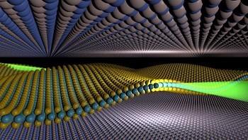
Two-dimensional materials such as graphene may only be one or two atoms thick but they are poised to power flexible electronics, revolutionize composites and even clean our water.
However, being this thin comes at a price: the functional properties we depend on will change if the material becomes contaminated.
Luckily, many 2D materials exhibit the ‘self-cleaning phenomenon’, meaning when different 2D materials are pressed together, stray molecules from the air and the lab are pushed out leaving large areas clear of impurities.
Since graphene’s isolation in 2004 a whole host of other 2D materials have been discovered each with a range of different properties.
When graphene and other 2D materials are combined, the potential of these new materials comes alive.
Layering stacks of 2D materials in a precisely chosen sequence can produce new materials called heterostructures that can be fine-tuned to achieve a specific purpose (from LEDs, to water purification, to high speed electronics).
These flat regions have yielded some of the most fascinating physics of our time. Now, the assumption that these areas are completely clean is under scrutiny.
Writing in Nano Letters a team of researchers at the National Graphene Institute at The University of Manchester have shown that even the gas within which the 2D material stacks are assembled can affect the structure and properties of the materials.
They found that for one class of 2D materials called the transition metal dichalcogenides (TMDCs), some had a very large gap between them and their neighbour; a distance unexplained by theoretical calculations done by Professsor Katsnelson and Dr Rudenko at Radboud University, Netherlands.
These observations all seemed to point to the presence of impurities between the 2D materials. To confirm this, 2D materials were stacked in a pure Argon gas atmosphere using a sealed chamber (known as a glove-box) in which the environment can be completely controlled.
Where previously the same material had given large gaps between neighbours, this time gave distances matching those predicted by theory for a clean interface free from impurities.
“By taking a side view of these sandwich structures we can see how these unique materials stick together and discover new secrets we have previously missed.”
Dr Sarah Haigh, who led the team of researchers who carried out this work said: “This sort of insight is changing how we build devices like LEDs and sensors from 2D materials. The properties of these devices were known to depend heavily on how and where we make them, and for the first time we have observed why.”
The consequences of this finding will directly impact on how we make graphene devices for future applications, showing that even the environment within which 2D material stacks are assembled affects the atomic structure and properties.
This research was funded by the UK Engineering and Physical Sciences Research Council (EPSRC) and its NOWNANO Doctoral Training Centre, the Royal Society, the US Defense Threat Reduction Agency, and ERC starter grant EvoluTEM.
Related video:
Share on:


Testimonial
"Our marketing partnership with I-Connect007 is already delivering. Just a day after our press release went live, we received a direct inquiry about our updated products!"
Rachael Temple - AlltematedSuggested Items
Curing and Verification in PCB Shadow Areas
09/17/2025 | Doug Katze, DymaxDesign engineers know a simple truth that often complicates electronics manufacturing: Light doesn’t go around corners. In densely populated PCBs, adhesives and coatings often fail to fully cure in shadowed regions created by tall ICs, connectors, relays, and tight housings.
September 2025 PCB007 Magazine: The Future of Advanced Materials
09/16/2025 | I-Connect007 Editorial TeamMoore’s Law is no more, and the advanced material solutions being developed to grapple with this reality are surprising, stunning, and perhaps a bit daunting. Buckle up for a dive into advanced materials and a glimpse into the next chapters of electronics manufacturing.
I-Connect007 Launches Advanced Electronics Packaging Digest
09/15/2025 | I-Connect007I-Connect007 is pleased to announce the launch of Advanced Electronics Packaging Digest (AEPD), a new monthly digital newsletter dedicated to one of the most critical and rapidly evolving areas of electronics manufacturing: advanced packaging at the interconnect level.
Panasonic Industry will Double the Production Capacity of MEGTRON Multi-layer Circuit Board Materials Over the Next Five Years
09/15/2025 | Panasonic Industry Co., Ltd.Panasonic Industry Co., Ltd., a Panasonic Group company, announced plans for a major expansion of its global production capacity for MEGTRON multi-layer circuit board materials today. The company plans to double its production over the next five years to meet growing demand in the AI server and ICT infrastructure markets.
Trouble in Your Tank: Implementing Direct Metallization in Advanced Substrate Packaging
09/15/2025 | Michael Carano -- Column: Trouble in Your TankDirect metallization systems based on conductive graphite are gaining popularity throughout the world. The environmental and productivity gains achievable with this process are outstanding. Direct metallization reduces the costs of compliance, waste treatment, and legal issues related to chemical exposure. A graphite-based direct plate system has been devised to address these needs.