


 Trouble in Your Tank: Implementing Direct Metallization in Advanced Substrate Packaging
 It’s Only Common Sense: Storytelling That Sells—Stop Pitching, Start Painting Pictures
 The Right Approach: Get Ready for ISO 9001 Version 6


New Optical Device Could Help Detect Drugs, Bomb-Making Chemicals and More
August 2, 2017 | University at BuffaloEstimated reading time: 2 minutes
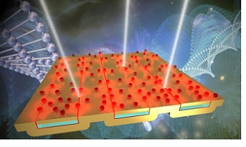
Scientists searching for traces of drugs, bomb-making components and other chemicals often shine light on the materials they’re analyzing. This approach is known as spectroscopy, and it involves studying how light interacts with trace amounts of matter.
One of the more effective types of spectroscopy is infrared absorption spectroscopy, which scientists use to sleuth out performance-enhancing drugs in blood samples and tiny particles of explosives in the air.
While infrared absorption spectroscopy has improved greatly in the last 100 years, researchers are still working to make the technology more sensitive, inexpensive and versatile. A new light-trapping sensor, developed by a University at Buffalo-led team of engineers and described in an Advanced Optical Materials study, makes progress in all three areas.
“This new optical device has the potential to improve our abilities to detect all sorts of biological and chemical samples,” says Qiaoqiang Gan, PhD, associate professor of electrical engineering in the School of Engineering and Applied Sciences at UB, and the study’s lead author.
Co-authors of the study — which will be featured on the cover of September’s Advanced Science News — in Gan’s lab include Dengxin Ji, Alec Cheney, Nan Zhang Haomin Song and Xie Zeng, PhD. Additional co-authors come from Fudan University and Northeastern University, both in China, and the University of Wisconsin-Madison.
The sensor works with light in the mid-infrared band of the electromagnetic spectrum. This part of the spectrum is used for most remote controls, night-vision and other applications.
The sensor consists of two layers of metal with an insulator sandwiched in between. Using a fabrication technique called atomic layer deposition, researchers created a device with gaps less than five nanometers (a human hair is roughly 75,000 nanometers in diameter) between two metal layers. Importantly, these gaps enable the sensor to absorb up to 81 percent of infrared light, a significant improvement from the 3 percent that similar devices absorb.
The process is known as surface-enhanced infrared absorption (SEIRA) spectroscopy. The sensor, which acts as a substrate for the materials being examined, boosts the sensitivity of SEIRA devices to detect molecules at 100 to 1,000 times greater resolution than previously reported results.
The increase makes SEIRA spectroscopy comparable to another type of spectroscopic analysis, surface-enhanced Rama spectroscopy (SERS), which measures light scattering as opposed to absorption.
The SEIRA advancement could be useful in any scenario that calls for finding traces of molecules, says Ji, the first author and a PhD candidate in Gan’s lab. This includes but is not limited to drug detection in blood, bomb-making materials, fraudulent art and tracking diseases.
Researchers plan to continue the research, and examine how to combine the SEIRA advancement with cutting-edge SERS.
The research is supported by the U.S. National Science Foundation’s Nanomanufacturing program, the National Science Foundation of China and the Chinese Scholarship Council.
Share on:


Testimonial
"Advertising in PCB007 Magazine has been a great way to showcase our bare board testers to the right audience. The I-Connect007 team makes the process smooth and professional. We’re proud to be featured in such a trusted publication."
Klaus Koziol - atgSuggested Items
Curing and Verification in PCB Shadow Areas
09/17/2025 | Doug Katze, DymaxDesign engineers know a simple truth that often complicates electronics manufacturing: Light doesn’t go around corners. In densely populated PCBs, adhesives and coatings often fail to fully cure in shadowed regions created by tall ICs, connectors, relays, and tight housings.
September 2025 PCB007 Magazine: The Future of Advanced Materials
09/16/2025 | I-Connect007 Editorial TeamMoore’s Law is no more, and the advanced material solutions being developed to grapple with this reality are surprising, stunning, and perhaps a bit daunting. Buckle up for a dive into advanced materials and a glimpse into the next chapters of electronics manufacturing.
I-Connect007 Launches Advanced Electronics Packaging Digest
09/15/2025 | I-Connect007I-Connect007 is pleased to announce the launch of Advanced Electronics Packaging Digest (AEPD), a new monthly digital newsletter dedicated to one of the most critical and rapidly evolving areas of electronics manufacturing: advanced packaging at the interconnect level.
Panasonic Industry will Double the Production Capacity of MEGTRON Multi-layer Circuit Board Materials Over the Next Five Years
09/15/2025 | Panasonic Industry Co., Ltd.Panasonic Industry Co., Ltd., a Panasonic Group company, announced plans for a major expansion of its global production capacity for MEGTRON multi-layer circuit board materials today. The company plans to double its production over the next five years to meet growing demand in the AI server and ICT infrastructure markets.
Trouble in Your Tank: Implementing Direct Metallization in Advanced Substrate Packaging
09/15/2025 | Michael Carano -- Column: Trouble in Your TankDirect metallization systems based on conductive graphite are gaining popularity throughout the world. The environmental and productivity gains achievable with this process are outstanding. Direct metallization reduces the costs of compliance, waste treatment, and legal issues related to chemical exposure. A graphite-based direct plate system has been devised to address these needs.