


 Trouble in Your Tank: Implementing Direct Metallization in Advanced Substrate Packaging
 It’s Only Common Sense: Storytelling That Sells—Stop Pitching, Start Painting Pictures
 The Right Approach: Get Ready for ISO 9001 Version 6


Scientists Watch ‘Artificial Atoms’ Assemble into Perfect Lattices with Many Uses
August 3, 2017 | SLAC National Accelerator LaboratoryEstimated reading time: 5 minutes
Some of the world’s tiniest crystals are known as “artificial atoms” because they can organize themselves into structures that look like molecules, including “superlattices” that are potential building blocks for novel materials.
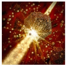
An illustration shows nanocrystals assembling into an ordered ‘superlattice’ – a process that a SLAC/Stanford team was able to observe in real time with X-rays from the Stanford Synchrotron Radiation Lightsource (SSRL). They discovered that this assembly takes just a few seconds when carried out in hot solutions. The results open the door for rapid self-assembly of nanocrystal building blocks into complex structures with applications in optoelectronics, solar cells, catalysis and magnetic materials. (Greg Stewart/SLAC National Accelerator Laboratory)
Now scientists from the Department of Energy’s SLAC National Accelerator Laboratory and Stanford University have made the first observation of these nanocrystals rapidly forming superlattices while they are themselves still growing. What they learn will help scientists fine-tune the assembly process and adapt it to make new types of materials for things like magnetic storage, solar cells, optoelectronics and catalysts that speed chemical reactions.
The key to making it work was the serendipitous discovery that superlattices can form superfast – in seconds rather than the usual hours or days – during the routine synthesis of nanocrystals. The scientists used a powerful beam of X-rays at SLAC’s Stanford Synchrotron Radiation Lightsource (SSRL) to observe the growth of nanocrystals and the rapid formation of superlattices in real time.
A paper describing the research, which was done in collaboration with scientists at the DOE’s Argonne National Laboratory, was published today in Nature.
“The idea is to see if we can get an independent understanding of how these superlattices grow so we can make them more uniform and control their properties,” said Chris Tassone, a staff scientist at SSRL who led the study with Matteo Cargnello, assistant professor of chemical engineering at Stanford.
Tiny Crystals with Outsized Properties
Scientists have been making nanocrystals in the lab since the 1980s. Because of their tiny size –they’re billionths of a meter wide and contain just 100 to 10,000 atoms apiece -- they are governed by the laws of quantum mechanics, and this gives them interesting properties that can be changed by varying their size, shape and composition. For instance, spherical nanocrystals known as quantum dots, which are made of semiconducting materials, glow in colors that depend on their size; they are used in biological imaging and most recently in high-definition TV displays.
In the early 1990s, researchers started using nanocrystals to build superlattices, which have the ordered structure of regular crystals, but with small particles in place of individual atoms. These, too, are expected to have unusual properties that are more than the sum of their parts.
But until now, superlattices have been grown slowly at low temperatures, sometimes in a matter of days.
That changed in February 2016, when Stanford postdoctoral researcher Liheng Wu serendipitously discovered that the process can occur much faster than scientists had thought.
‘Something Weird Is Happening’
He was trying to make nanocrystals of palladium - a silvery metal that’s used to promote chemical reactions in catalytic converters and many industrial processes – by heating a solution containing palladium atoms to more than 230 degrees Celsius. The goal was to understand how these tiny particles form, so their size and other properties could be more easily adjusted.
The team added small windows to a reaction chamber about the size of a tangerine so they could shine an SSRL X-ray beam through it and watch what was happening in real time.
“It’s kind of like cooking,” Cargnello explained. “The reaction chamber is like a pan. We add a solvent, which is like the frying oil; the main ingredients for the nanocrystals, such as palladium; and condiments, which in this case are surfactant compounds that tune the reaction conditions so you can control the size and composition of the particles. Once you add everything to the pan, you heat it up and fry your stuff.”
Wu and Stanford graduate student Joshua Willis expected to see the characteristic pattern made by X-rays scattering off the tiny particles. They saw a completely different pattern instead.
“So something weird is happening,” they texted their adviser.
The something weird was that the palladium nanocrystals were assembling into superlattices.
A Balance of Forces
At this point, “The challenge was to understand what brings the particles together and attracts them to each other but not too strongly, so they have room to wiggle around and settle into an ordered position,” said Jian Qin, an assistant professor of chemical engineering at Stanford who performed theoretical calculations to better understand the self-assembly process.
Once the nanocrystals form, what seems to be happening is that they acquire a sort of hairy coating of surfactant molecules. The nanocrystals glom together, attracted by weak forces between their cores, and then a finely tuned balance of attractive and repulsive forces between the dangling surfactant molecules holds them in just the right configuration for the superlattice to grow.
To the scientists’ surprise, the individual nanocrystals then kept on growing, along with the superlattices, until all the chemical ingredients in the solution were used up, and this unexpected added growth made the material swell. The researchers said they think this occurs in a wide range of nanocrystal systems, but had never been seen because there was no way to observe it in real time before the team’s experiments at SSRL.
“Once we understood this system, we realized this process may be more general than we initially thought,” Wu said. “We have demonstrated that it’s not only limited to metals, but it can also be extended to semiconducting materials and very likely to a much larger set of materials.”
The team has been doing follow-up experiments to find out more about how the superlattices grow and how they can tweak the size, composition and properties of the finished product.
Ian Salmon McKay, a graduate student in chemical engineering at Stanford, and Benjamin T. Diroll, a postdoctoral researcher at Argonne National Laboratory’s Center for Nanoscale Materials (CNM), also contributed to the work.
SSRL and CNM are DOE Office of Science User Facilities. The research was funded by the DOE Office of Science and by a Laboratory Directed Research and Development grant from SLAC.
Share on:


Testimonial
"Advertising in PCB007 Magazine has been a great way to showcase our bare board testers to the right audience. The I-Connect007 team makes the process smooth and professional. We’re proud to be featured in such a trusted publication."
Klaus Koziol - atgSuggested Items
Meet the Author Podcast: Martyn Gaudion Unpacks the Secrets of High-Speed PCB Design
07/16/2025 | I-Connect007In this special Meet the Author episode of the On the Line with… podcast, Nolan Johnson sits down with Martyn Gaudion, signal integrity expert, managing director of Polar Instruments, and three-time author in I-Connect007’s popular The Printed Circuit Designer’s Guide to... series.
Intervala Hosts Employee Car and Motorcycle Show, Benefit Nonprofits
08/27/2024 | IntervalaIntervala hosted an employee car and motorcycle show, aptly named the Vala-Cruise and it was a roaring success! Employees had the chance to show off their prized wheels, and it was incredible to see the variety and passion on display.
KIC Honored with IPC Recognition for 25 Years of Membership and Contributions to Electronics Manufacturing Industry
06/24/2024 | KICKIC, a renowned pioneer in thermal process and temperature measurement solutions for electronics manufacturing, is proud to announce that it has been recognized by IPC for 25 years of membership and significant contributions to electronics manufacturing.
Boeing Starliner Spacecraft Completes Successful Crewed Docking with International Space Station
06/07/2024 | BoeingNASA astronauts Barry "Butch" Wilmore and Sunita "Suni" Williams successfully docked Boeing's Starliner spacecraft to the International Space Station (ISS), about 26 hours after launching from Cape Canaveral Space Force Station.
KIC’s Miles Moreau to Present Profiling Basics and Best Practices at SMTA Wisconsin Chapter PCBA Profile Workshop
01/25/2024 | KICKIC, a renowned pioneer in thermal process and temperature measurement solutions for electronics manufacturing, announces that Miles Moreau, General Manager, will be a featured speaker at the SMTA Wisconsin Chapter In-Person PCBA Profile Workshop.