


 It’s Only Common Sense: The Underrated Business Strategy of Joy
 Punching Out: How to Stay Focused in Business and M&A


Design and nanomanufacturing have collided inside of a Northwestern University laboratory.
An interdisciplinary team of researchers has used mathematics and machine learning to design an optimal material for light management in solar cells, then fabricated the nanostructured surfaces simultaneously with a new nanomanufacturing technique.
“We have bridged the gap between design and nanomanufacturing,” said Wei Chen, the Wilson-Cook Professor in Engineering Design and professor of mechanical engineering in Northwestern’s McCormick School of Engineering, who led the study’s design component. “Instead of designing a structure element by element, we are now designing and optimizing it with a simple mathematic function and fabricating it at the same time.”
The fast, highly scalable, streamlined method could replace cumbersome trial-and-error nanomanufacturing and design methods, which often take vast resources to complete.
“The concurrent design and processing of nanostructures paves the way to avoid trial-and-error manufacturing, increasing the cost effectiveness to prototype nanophotonic devices,” said Teri Odom, Charles E. and Emma H. Morrison Professor of Chemistry in Northwestern’s Weinberg College of Arts and Sciences and leader of the study’s nanofabrication component.
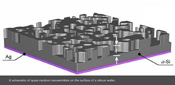
Researchers are currently interested in nanophotonic materials for light absorption in ultra-thin, flexible solar cells. The same principle could also be applied to implement color into clothing without dyes and to create anti-wet surfaces. For solar cells, the ideal nanostructure surface features quasi-random structures — meaning the structures appear random but do have a pattern. Designing these patterns can be difficult and time consuming, since there are thousands of geometric variables that must be optimized simultaneously to discover the optimal surface pattern to absorb the most light.
“It is a very tedious job to fabricate the optimal design,” Chen said. “You could use nano-lithography, which is similar to 3D printing, but it takes days and thousands of dollars just to print a little square. That’s not practical.”
To bypass the issues of nano-lithography, Odom and Chen manufactured the quasi-random structures with wrinkle lithography, a new nanomanufacturing technique that can rapidly transfer wrinkle patterns into different materials to realize a nearly unlimited number of quasi-random nanostructures. Formed by applying strain to a substrate, wrinkling is a simple method for the scalable fabrication of nanoscale surface structures.
“Importantly, the complex geometries can be described computationally with only three parameters — instead of thousands typically required by other approaches,” Odom said. “We then used the digital designs in an iterative search loop to determine the optimal nanowrinkles for a desired outcome.”
Supported by the National Science Foundation and Office of Naval Research, the research was published online this week in the Proceedings of the National Academy of Sciences. Won-Kyu Lee, a PhD student in Odom’s laboratory, served as the paper’s first author. Shuangcheng Yu, a PhD student who recently graduated from Chen’s Integrated Design Automation Laboratory (IDEAL), served as the paper’s second author. Lee and Yu contributed equally to the work.
The team demonstrated the concurrent design and manufacturing method to fabricate 3D photonic nanostructures on a silicon wafer for potential use as a solar cell. The resulting material absorbed 160 percent more light in the 800 to 1,200 nanometer wavelength — a range in which current solar cells are less efficient — than other designs.
“Light wavelengths have different frequencies, and we did not design for just one frequency,” Chen said. “We designed for the whole spectrum of sunlight frequencies, so the solar cell can absorb light over broadband wavelengths and over a wide collection of angles.”
Next, the team plans to apply its method to other materials, such as polymers, metals, and oxides, for other photonics applications.
Original by: Amanda Morris


