


 Trouble in Your Tank: Implementing Direct Metallization in Advanced Substrate Packaging
 It’s Only Common Sense: Storytelling That Sells—Stop Pitching, Start Painting Pictures
 The Right Approach: Get Ready for ISO 9001 Version 6


Scientists Find New Method to Control Electronic Properties of Nanocrystals
August 11, 2017 | Brookhaven National LaboratoryEstimated reading time: 4 minutes
Researchers from The Hebrew University of Jerusalem, Stony Brook University, and the U.S. Department of Energy's (DOE) Brookhaven National Laboratory have discovered new effects of an important method for modulating semiconductors. The method, which works by creating open spaces or "vacancies" in a material's structure, enables scientists to tune the electronic properties of semiconductor nanocrystals (SCNCs)—semiconductor particles that are smaller than 100 nanometers. This finding will advance the development of new technologies like smart windows, which can change opaqueness on demand.
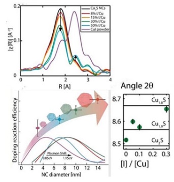
(Top) The removal of copper from copper sulfide nanocrystals and the growth of copper iodine on nanocrystal facets is depicted by results from XAFS; (Bottom left) Larger nanocrystals are doped more efficiently by vacancy formation; (Right) Vacancy formation is observed by XRD
Scientists use a technique called "chemical doping" to control the electronic properties of semiconductors. In this process, chemical impurities—atoms from different materials—are added to a semiconductor in order to alter its electrical conductivity. Though it is possible to dope SCNCs, it is very difficult due to their tiny size. The amount of impurities added during chemical doping is so small that in order to dope a nanocrystal properly, no more than a few atoms can be added to the crystal. Nanocrystals also tend to expel impurities, further complicating the doping process.
Seeking to control the electronic properties of SCNCs more easily, researchers studied a technique called vacancy formation. In this method, impurities are not added to the semiconductor; instead, vacancies in its structure are formed by oxidation-reduction (redox) reactions, a type of chemical reaction where electrons are transferred between two materials. During this transfer, a type of doping occurs as missing electrons, called holes, become free to move throughout the structure of the crystal, significantly altering the electrical conductivity of the SCNC.
From Left to Right: XPD beamline scientist Sanjit Ghose, postdoctoral researcher Anna Plonka, and Brookhaven Chemist Anatoly Frenkel.
"We have also identified size effects in the efficiency of the vacancy formation doping reaction," said Uri Banin, a nanotechnologist from the Hebrew University of Jerusalem. "Vacancy formation is actually more efficient in larger SCNCs."
In this study, the researchers investigated a redox reaction between copper sulfide nanocrystals (the semiconductor) and iodine, a chemical introduced in order to influence the redox reaction to occur.
"If you reduce copper sulfide, you will pull out copper from the nanocrystal, generating vacancies and therefore holes," said Anatoly Frenkel, a chemist at Brookhaven National Laboratory holding a joint appointment with Stony Brook University, and the lead Brookhaven researcher on this study.
The researchers used the x-ray powder diffraction (XPD) beamline at the National Synchrotron Light Source II (NSLS-II)—a DOE Office of Science User Facility—to study the structure of copper sulfide during the redox reaction. By shining ultra-bright x-rays onto their samples, the researchers are able to determine the amount of copper that is pulled out during the redox reaction.
Based on their observations at NSLS-II, the team confirmed that adding more iodine to the system caused more copper to be released and more vacancies to form. This established that vacancy formation is a useful technique for tuning the electronic properties of SCNCs.
Still, the researchers needed to find out what exactly was happening to copper when it left the nanocrystal. Understanding how copper behaves after the redox reaction is crucial for implementing this technique into smart window technology.
"If copper uncontrollably disappears, we can't pull it back into the system," Frenkel said. "But suppose the copper that is taken out of the crystal is hovering around, ready to go back in. By using the reverse process, we can put it back into the system, and we can make a device that would be easy to switch from one state to the other. For example, you would be able to change the transparency of a window on demand, depending on the time of day or your mood."
To understand what was happening to copper, the researchers used x-ray absorption fine structure (XAFS) spectroscopy at the Advanced Photon Source (APS)—also a DOE Office of Science User Facility—at Argonne National Laboratory. This technique allows the researchers to study the extremely small copper complexes that x-ray diffraction cannot detect. XAFS revealed that copper was combining with iodine to form copper iodine, a positive result that indicated copper could be put back into the nanocrystal and that the researchers have full control of the electronic properties.
The researchers say the next step is to study materials in real-time during redox reactions using NSLS-II.
This study was supported by the National Science Foundation, the US-Israel Binational Science Foundation, and Northwestern University. DOE's Office of Science also supports operations at NSLS-II and APS.
Brookhaven National Laboratory is supported by the Office of Science of the U.S. Department of Energy. The Office of Science is the single largest supporter of basic research in the physical sciences in the United States, and is working to address some of the most pressing challenges of our time. For more information, please visit science.energy.gov.
Share on:


Testimonial
"The I-Connect007 team is outstanding—kind, responsive, and a true marketing partner. Their design team created fresh, eye-catching ads, and their editorial support polished our content to let our brand shine. Thank you all! "
Sweeney Ng - CEE PCBSuggested Items
Trouble in Your Tank: Implementing Direct Metallization in Advanced Substrate Packaging
09/15/2025 | Michael Carano -- Column: Trouble in Your TankDirect metallization systems based on conductive graphite are gaining popularity throughout the world. The environmental and productivity gains achievable with this process are outstanding. Direct metallization reduces the costs of compliance, waste treatment, and legal issues related to chemical exposure. A graphite-based direct plate system has been devised to address these needs.
Closing the Loop on PCB Etching Waste
09/09/2025 | Shawn Stone, IECAs the PCB industry continues its push toward greener, more cost-efficient operations, Sigma Engineering’s Mecer System offers a comprehensive solution to two of the industry’s most persistent pain points: etchant consumption and rinse water waste. Designed as a modular, fully automated platform, the Mecer System regenerates spent copper etchants—both alkaline and acidic—and simultaneously recycles rinse water, transforming a traditionally linear chemical process into a closed-loop system.
Driving Innovation: Depth Routing Processes—Achieving Unparalleled Precision in Complex PCBs
09/08/2025 | Kurt Palmer -- Column: Driving InnovationIn PCB manufacturing, the demand for increasingly complex and miniaturized designs continually pushes the boundaries of traditional fabrication methods, including depth routing. Success in these applications demands not only on robust machinery but also sophisticated control functions. PCB manufacturers rely on advanced machine features and process methodologies to meet their precise depth routing goals. Here, I’ll explore some crucial functions that empower manufacturers to master complex depth routing challenges.
Trouble in Your Tank: Minimizing Small-via Defects for High-reliability PCBs
08/27/2025 | Michael Carano -- Column: Trouble in Your TankTo quote the comedian Stephen Wright, “If at first you don’t succeed, then skydiving is not for you.” That can be the battle cry when you find that only small-diameter vias are exhibiting voids. Why are small holes more prone to voids than larger vias when processed through electroless copper? There are several reasons.
The Government Circuit: Navigating New Trade Headwinds and New Partnerships
08/25/2025 | Chris Mitchell -- Column: The Government CircuitAs global trade winds continue to howl, the electronics manufacturing industry finds itself at a critical juncture. After months of warnings, the U.S. Government has implemented a broad array of tariff increases, with fresh duties hitting copper-based products, semiconductors, and imports from many nations. On the positive side, tentative trade agreements with Europe, China, Japan, and other nations are providing at least some clarity and counterbalance.