


 Trouble in Your Tank: Implementing Direct Metallization in Advanced Substrate Packaging
 It’s Only Common Sense: Storytelling That Sells—Stop Pitching, Start Painting Pictures
 The Right Approach: Get Ready for ISO 9001 Version 6


Fewer Defects from a 2D Approach
August 14, 2017 | KAUSTEstimated reading time: 2 minutes
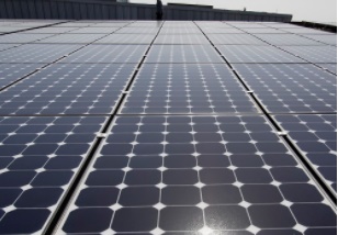
Improving the efficiency of solar cells requires materials free from impurities and structural defects. Scientists across many disciplines at KAUST have shown that 2D organic-inorganic hybrid materials feature far fewer defects than thicker 3D versions.
Modern-day electronics rely on technologies that can develop almost perfect crystals of silicon; flawless to the atomic level. This is crucial because defects and impurities scatter electrons as they flow, which adversely affects the material’s electronic properties.
But hybrid perovskites, an exciting class of electronic material, cannot be constructed using the epitaxial or layer methods developed for silicon. Instead, they are produced using solution-based processes. While this makes them cheaper than silicon, it also makes purity much harder to achieve as defect population and species are sensitive to the processing conditions.
Osman Bakr from the KAUST Solar Center together with colleagues from multiple divisions across KAUST and the University of Toronto, demonstrate that two-dimensional layers of perovskite material can achieve levels of purity much higher than is possible than in their 3D counterpart. “Two-dimensional hybrid perovskites are a subgroup of the big hybrid perovskite family,” explains Wei Peng, lead author and doctoral degree recipient from Bakr’s lab. “They can be derived by inserting large organic cations in three-dimensional perovskite structures.”
Hybrid perovskites are made up of lead and halide (such as iodine) atoms and an organic component. This class of materials in solar cells has already shown ground-breaking potential for energy conversion efficiency while having low production costs and the possibility for being integrated in flexible devices. This combination of qualities makes hybrid perovskites an exciting material for optoelectronic applications.
Peng, Bakr and coworkers created a 2D material made of periodic layers of hybrid perovskites with an organic component of either phenethylammonium or methylammonium. Using a solution-based fabrication method, the layers were placed on a gold electrode so the team could measure the electrical conductivity.
Their measurements indicate that the 2D materials contained three orders of magnitude fewer defects than bulk hybrid perovskites. The team proposes that this reduction is because the large organic cations in the phenethylammonium suppress defect formation during crystallization.
Next, the team demonstrated the potential for their materials for optoelectronic applications by constructing photoconductors with high light detectivity. These results bode well for further advancements in designing and optimizing perovskite solar cells. “A future in-depth study on how the defect formation is suppressed will help our understanding and benefit device performance-targeted materials engineering,” says Peng.
Share on:


Testimonial
"Advertising in PCB007 Magazine has been a great way to showcase our bare board testers to the right audience. The I-Connect007 team makes the process smooth and professional. We’re proud to be featured in such a trusted publication."
Klaus Koziol - atgSuggested Items
September 2025 PCB007 Magazine: The Future of Advanced Materials
09/16/2025 | I-Connect007 Editorial TeamMoore’s Law is no more, and the advanced material solutions being developed to grapple with this reality are surprising, stunning, and perhaps a bit daunting. Buckle up for a dive into advanced materials and a glimpse into the next chapters of electronics manufacturing.
I-Connect007 Launches Advanced Electronics Packaging Digest
09/15/2025 | I-Connect007I-Connect007 is pleased to announce the launch of Advanced Electronics Packaging Digest (AEPD), a new monthly digital newsletter dedicated to one of the most critical and rapidly evolving areas of electronics manufacturing: advanced packaging at the interconnect level.
Panasonic Industry will Double the Production Capacity of MEGTRON Multi-layer Circuit Board Materials Over the Next Five Years
09/15/2025 | Panasonic Industry Co., Ltd.Panasonic Industry Co., Ltd., a Panasonic Group company, announced plans for a major expansion of its global production capacity for MEGTRON multi-layer circuit board materials today. The company plans to double its production over the next five years to meet growing demand in the AI server and ICT infrastructure markets.
Trouble in Your Tank: Implementing Direct Metallization in Advanced Substrate Packaging
09/15/2025 | Michael Carano -- Column: Trouble in Your TankDirect metallization systems based on conductive graphite are gaining popularity throughout the world. The environmental and productivity gains achievable with this process are outstanding. Direct metallization reduces the costs of compliance, waste treatment, and legal issues related to chemical exposure. A graphite-based direct plate system has been devised to address these needs.
Fresh PCB Concepts: Designing for Success at the Rigid-flex Transition Area
08/28/2025 | Team NCAB -- Column: Fresh PCB ConceptsRigid-flex PCBs come in all shapes and sizes. Manufacturers typically use fire-retardant, grade 4 (FR-4) materials in the rigid section and flexible polyimide materials in the flex region. Because of the small size, some rigid-flex PCBs, like those for hearing aid devices, are among the most challenging to manufacture. However, regardless of its size, we should not neglect the transition area between the rigid and flexible material.