


 Trouble in Your Tank: Implementing Direct Metallization in Advanced Substrate Packaging
 It’s Only Common Sense: Storytelling That Sells—Stop Pitching, Start Painting Pictures
 The Right Approach: Get Ready for ISO 9001 Version 6


Scientists Shine New Light on the 'Other High Temperature Superconductor'
August 15, 2017 | CUIEstimated reading time: 2 minutes
A study led by scientists of the Max Planck Institute for the Structure and Dynamics of Matter (MPSD) presents evidence of the coexistence of superconductivity and “charge-density-waves” in compounds of the poorly-studied family of bismuthates. This observation opens up new perspectives for a deeper understanding of the phenomenon of high-temperature superconductivity, a topic which has been at the core of condensed matter research for more than 30 years.
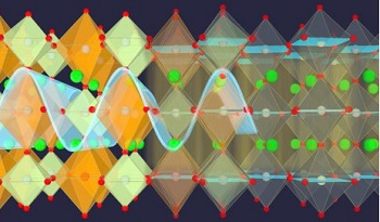
Intense laser pulses were used to photo-excite bismuthate compounds, in which “charge-density-waves” (left side) coexist with superconductivity (right side). J.M. Harms, MPSD
In the study, which has just been published in PNAS, the scientists around CUI member Prof. Andrea Cavalleri and Dr. Daniele Nicoletti focused on different compounds, belonging to the poorly studied family of bismuthates. These superconductors were discovered in the 1970s, even before the cuprates, the best known and heavily studied family of high temperature superconductor. Due to their far lower critical temperatures (about 30 K), however, bismuthates attracted less attention. They share many commonalities, but also some differences with their better-known relatives. In particular, the so-called “parent compound” BaBiO3 has a robust charge-density-wave phase, from which superconductivity emerges by chemical substitution.
High quality crystals of BaPb1-xBixO3, with different Pb concentrations “x”, were synthetized and characterized by Ian R. Fisher and P. Giraldo-Gallo at Stanford University, California. The MPSD team from the Center for Free-Electron Laser Science in Hamburg performed a series of experiments on these crystals, in which they photo-excited the materials with very short and intense laser pulses and measured how their conductivity was transiently modified and relaxed back to the initial value within few picoseconds. By analyzing the dependence of such signal on frequency, temperature, and Pb concentration, they could uniquely assign it to a modification of the charge-density-wave phase induced by the laser field.
Indirect demonstration of coexistence
“Strikingly,” says Nicoletti, “we were able to measure this response not only in the parent compound BaBiO3, for which a charge-density-wave is well known to exist, but also in a Pb-doped superconducting compound. This observation is an indirect demonstration of the coexistence of charge-density-waves and superconductivity in the very same material, something that has been discussed previously, but never definitely established in this class of materials.”
The scientists were also able to exactly determine the energy scales associated with the modification of the charge-density-waves, thus providing new information on their dynamical interplay with superconductivity in bismuthates.
These results are especially timely given that charge-density-waves have recently been found in several cuprate superconductors, pointing towards a surprising commonality between some aspects of these materials. The present experiment is an additional example of how light can be employed to investigate, control, and manipulate complex materials. One of the ultimate goals of this line of research is to provide guidance for material engineering to develop new functionalities at increasingly higher temperatures.
Share on:


Testimonial
"Our marketing partnership with I-Connect007 is already delivering. Just a day after our press release went live, we received a direct inquiry about our updated products!"
Rachael Temple - AlltematedSuggested Items
Electra’s ElectraJet EMJ110 Inkjet Soldermask Now in Black & Blue at Sunrise Electronics
09/08/2025 | Electra Polymers LtdFollowing the successful deployment of Electra’s Green EMJ110 Inkjet Soldermask on KLA’s Orbotech Neos™ platform at Sunrise Electronics in Elk Grove Village, Illinois, production has now moved beyond green.
Magnachip Semiconductor Announces YJ Kim to Step Down as CEO; Current Board Chairman Camillo Martino Appointed Interim CEO
08/14/2025 | PR NewswireMagnachip Semiconductor Corporation today announced that YJ Kim has agreed to step down as CEO and as a member of the Board of Directors, effective immediately. Camillo Martino, Chairman of the Board of Directors, has also been appointed Interim Chief Executive Officer, effective immediately.
Bell to Build X-Plane for Phase 2 of DARPA Speed and Runway Independent Technologies (SPRINT) X-Plane Program
07/09/2025 | Bell Textron Inc.Bell Textron Inc., a Textron Inc. company, has been down-selected for Phase 2 of Defense Advanced Research Projects Agency (DARPA) Speed and Runway Independent Technologies (SPRINT) X-Plane program with the objective to complete design, construction, ground testing and certification of an X-plane demonstrator.
Nolan’s Notes: Moving Forward With Confidence
06/03/2025 | Nolan Johnson -- Column: Nolan's NotesWe’re currently enjoying a revitalized and dynamic EMS provider market with significant growth potential. Since December 2024, the book-to-bill has been extremely strong and growing. Starting with a ratio of 1.24 in December, book-to-bill has continued to accelerate to a 1.41 in April. Yet, there is a global economic restructuring taking place. To say that the back-and-forth with tariffs and trade deals makes for an uncertain market is an understatement. While we may be in a 90-day tariff pause among leading economic nations, the deadline is quickly approaching and that leaves many of you feeling unsettled about what to expect.
Mycronic High Flex Changes Division Name to PCB Assembly Solutions
05/20/2025 | MycronicMycronic AB, the leading Sweden-based electronics assembly solutions provider, announced that its division formerly known as High Flex will now operate under the name PCB Assembly Solutions.