


 Trouble in Your Tank: Implementing Direct Metallization in Advanced Substrate Packaging
 It’s Only Common Sense: Storytelling That Sells—Stop Pitching, Start Painting Pictures
 The Right Approach: Get Ready for ISO 9001 Version 6


Researchers Printed Graphene-Like Materials with Inkjet
August 18, 2017 | Aalto UniversityEstimated reading time: 2 minutes
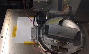
An international research team has developed inks made of graphene-like materials for inkjet printing. New black phosphorous inks are compatible with conventional inkjet printing techniques for optoelectronics and photonics.
New black phosphorous inks are compatible with conventional inkjet printing techniques for optoelectronics and photonics.
Since the discovery of the Nobel Prize winning material graphene, many new nanomaterials promise to deliver exciting new photonic and optoelectronic technologies. Black phosphorous is a particularly interesting post-graphene nanomaterial for next generation photonic and optoelectronic devices. Yet despite remarkable performance in the lab, practical real-world exploitation of this material has been hindered by complex material fabrication and its poor environmental stability. “Our inkjet printing demonstration makes possible for the first time the scalable mass fabrication of black phosphorous based photonic and optoelectronic devices with long-term stability necessary for a wide range of industrial applications”, tells Professor Zhipei Sun at Aalto University in Finland.
Scientists optimized the chemical composition to achieve a stable ink through the balance of complex and competing fluidic effects. This enabled the production of new functional photonic and optoelectronic devices by inkjet printing with excellent print quality and uniformity - just like the printing of intricate graphics or photographs on paper. The researchers' work demonstrated the benefits of their novel technique by inkjet printing devices that take advantage of the properties of black phosphorous, not least its semiconducting bandgap that can be readily varied by engineering the number of atomic layers and can cover the visible and near-infrared region of the electromagnetic spectrum.
The researchers also demonstrated printed black phosphorous based nonlinear optical devices that can be easily inserted into lasers to act as ultra-quick optical shutters, converting a continuous beam of laser radiation into a repetitive series of very short bursts of light suited for industrial and medical applications, such as machining, imaging and sensing. In the study, black phosphorous was also able to act as an efficient and highly-responsive detector of light, extending the wavelength range over which conventional silicon-based photodetectors can operate.
Importantly, the researchers showed that the black phosphorous ink can be seamlessly integrated with existing complementary metal-oxide-semiconductor (CMOS) technologies, while the inkjet printing technique developed offering the prospect of supporting the fabrication of so-called heterostructured materials that aim to capitalize on the benefits of distinct, yet complementary properties of multiple nanomaterial layers through controlled fabrication.
The new ink was developed by an interdisciplinary team of international researchers at Aalto University, University of Cambridge (UK), Imperial College London (UK) and Beihang University (China). The research was supported by the Academy of Finland, Tekes - the Finnish Funding Agency for Innovation, Nokia Foundation and European Commission.
Share on:


Testimonial
"Advertising in PCB007 Magazine has been a great way to showcase our bare board testers to the right audience. The I-Connect007 team makes the process smooth and professional. We’re proud to be featured in such a trusted publication."
Klaus Koziol - atgSuggested Items
MEMS & Imaging Sensors Summit to Spotlight Sensing Revolution for Europe’s Leadership
09/11/2025 | SEMIIndustry experts will gather November 19-20 at the SEMI MEMS & Imaging Sensors Summit 2025 to explore the latest breakthroughs in AI-driven MEMS and imaging optimization, AR/VR technologies, and advanced sensor solutions for critical defence applications.
Direct Imaging System Market Size to Hit $4.30B by 2032, Driven by Increasing Demand for High-Precision PCB Manufacturing
09/11/2025 | Globe NewswireAccording to the SNS Insider, “The Direct Imaging System Market size was valued at $2.21 Billion in 2024 and is projected to reach $4.30 Billion by 2032, growing at a CAGR of 8.68% during 2025-2032.”
I-Connect007’s Editor’s Choice: Five Must-Reads for the Week
07/04/2025 | Marcy LaRont, I-Connect007For our industry, we have seen several bullish market announcements over the past few weeks, including one this week by IDC on the massive growth in the global server market. We’re also closely watching global trade and nearshoring. One good example of successful nearshoring is Rehm Thermal Systems, which celebrates its 10th anniversary in Mexico and the official opening of its new building in Guadalajara.
Driving Innovation: Direct Imaging vs. Conventional Exposure
07/01/2025 | Simon Khesin -- Column: Driving InnovationMy first camera used Kodak film. I even experimented with developing photos in the bathroom, though I usually dropped the film off at a Kodak center and received the prints two weeks later, only to discover that some images were out of focus or poorly framed. Today, every smartphone contains a high-quality camera capable of producing stunning images instantly.
United Electronics Corporation Advances Manufacturing Capabilities with Schmoll MDI-ST Imaging Equipment
06/24/2025 | United Electronics CorporationUnited Electronics Corporation has successfully installed the advanced Schmoll MDI-ST (XL) imaging equipment at their advanced printed circuit board facility. This significant technology investment represents a continued commitment to delivering superior products and maintaining their position as an industry leader in precision PCB manufacturing.