


 Trouble in Your Tank: Implementing Direct Metallization in Advanced Substrate Packaging
 It’s Only Common Sense: Storytelling That Sells—Stop Pitching, Start Painting Pictures
 The Right Approach: Get Ready for ISO 9001 Version 6


Ten Billion Atoms in Rank and File
August 25, 2017 | TUMEstimated reading time: 4 minutes
Each atomic layer thin, tear-resistant, and stable. Graphene is seen as the material of the future. It is ideal for e.g. producing ultra-light electronics or highly stable mechanical components. But the wafer-thin carbon layers are difficult to produce. At the Technical University of Munich (TUM), Jürgen Kraus has manufactured self-supporting graphene membranes, and at the same time systematically investigated and optimized the growth of the graphene crystals. He was awarded the Evonik Research Prize for his work.
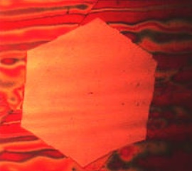
Visible to the naked eye: A wafer-thin graphene flake obtained via chemical vapor deposition. The red coloration of the copper substrate appears when the sample is heated in air. (Photo: J. Kraus/ TUM)
Graphene breaks all records. It is the thinnest and most stable material in the world, ultralight, tear-proof, electrically conductive, and highly resilient. Since it was discovered in 2004, the two-dimensional structures composed of carbon atoms have fueled the imagination and inventive spirit. Science fiction authors consider the material suitable for building cables to drive space elevators. Material researchers are experimenting with graphene displays, transistors, and electrodes, which purport to make the electronics of the future lighter, more stable, and longer-lived. In the scientific community, films of highly pure graphene are highly coveted, as they allow gases and liquids to be packaged in an ultra-dense manner.
"Currently, however, the basic requirements are still lacking. There are various manufacturing processes which are suitable for the mass production of graphene. However, this material is not free of defects. Graphene of the highest crystalline quality cannot be reproducibly manufactured in this manner", explains Sebastian Günther, Professor for Physical Chemistry at the TUM. His team has now succeeded in analyzing, monitoring, and optimizing the growth of graphene crystals through chemical vapor deposition (CVD for short). The findings were recently published in the "Annalen der Physik" (Annals of Physics).
Theory and caveats in practice
Theoretically, it is very easy to produce graphene: All that is needed are a heated glass vessel, a reactor, in which carbon-containing gas such as methane is fed into, as well as copper as a catalyst. At temperatures of around 1,000 degrees Celsius, the methane decomposes on the copper surface to produce hydrogen and carbon. While the hydrogen subsequently leaves the copper surface, the carbon atoms collect on the surface of the copper film used during this chemical precipitation from the gaseous state — a process called chemical vapor deposition. Here, the atoms cross-link and form graphene "flakes", spot-like two-dimensional structures with the typical honeycombed structure. What remains is the hydrogen, which can be extracted via suction.
However, in practice, the devil is in the details. "The biggest problem is that the two-dimensional crystal structure is often not entirely homogeneous, because growth begins simultaneously at multiple locations", explains Jürgen Kraus, who carried out the experiments. "At first glance, it appears that a continuous graphene film is appearing on the copper, but the hexagonal honeycombs are not all oriented in the same manner, and the structure is weakened at locations where they meet."
Such defects can be avoided by ensuring that the surface of the copper is as free of crystallization nuclei as possible.
With his experiments, the chemist was able to demonstrate that contaminants could best be removed with the help of oxygen gas — i.e. through oxidation. However, in order to avoid undesirable side effects, care must be taken to ensure that the copper catalyst is only exposed to the minimum possible amounts of oxygen.
Crucial for success: Gas concentration and temperature
In the second part of his experiments, Kraus analyzed how various partial pressures and temperatures affect the formation of graphene during chemical vapor deposition. If the gas composition used contains too much hydrogen, no graphene grows at all; if it has too little hydrogen, the layers become too thick. It is only when all parameters are selected such that growth occurs "close enough" to the thermal equilibrium that highly pure graphene without defects is formed in a crystal lattice.
Quality check in Italy
In order to verify the quality of the flakes, the Munich-based researchers took a trip to Italy with their samples. At the Research Centre Elettra Sincrotrone Trieste, which is equipped with a ring-shaped particle accelerator, they were able to chemically and structurally characterize the graphene layers with a special microscope, which had a high resolution thanks to the high-energy synchrotron radiation.
"The results of the feasibility study were highly encouraging", reports Günther. "The images have shown that reproducible results can be obtained by selecting the parameters during chemical vapor deposition"
The TUM researchers' best record for quality so far: Graphene flakes measuring one square millimeter containing ten billion precisely aligned carbon atoms. "The advantage over other studies is not so much the 'record size' achieved, but lies in the fact that the flakes are formed with a predictable growth rate if the right CVD parameters are chosen, thereby allowing closed, highly crystalline graphene layers with a thickness of just one atom to be manufactured within just a few hours", summarizes Günther.
Mini films for new applications
Graphene opens up a wide range of new applications, above all in basic research: For one, the ultra-thin graphene films can e.g. be removed from the copper substrate and used as covering films. Such films are suitable for trapping liquids in a container. Because the films are transparent to slow electrons, the samples can be studied via electron spectroscopy and microscopy, even though these techniques are typically used in ultra-high vacuums or high vacuums.
With the help of the films, the researchers also intend to investigate living cells, liquid-covered electrodes and catalysts under high pressure via photoelectron spectroscopy in the future. In this process, photons, which are able to penetrate the film, transfer their energy to the electrons in the sample, such that they are released and pass through the film to the outside. Their energy levels can then be used to derive conclusions regarding the chemical composition of the sample.
Share on:


Testimonial
"In a year when every marketing dollar mattered, I chose to keep I-Connect007 in our 2025 plan. Their commitment to high-quality, insightful content aligns with Koh Young’s values and helps readers navigate a changing industry. "
Brent Fischthal - Koh YoungSuggested Items
Trouble in Your Tank: Implementing Direct Metallization in Advanced Substrate Packaging
09/15/2025 | Michael Carano -- Column: Trouble in Your TankDirect metallization systems based on conductive graphite are gaining popularity throughout the world. The environmental and productivity gains achievable with this process are outstanding. Direct metallization reduces the costs of compliance, waste treatment, and legal issues related to chemical exposure. A graphite-based direct plate system has been devised to address these needs.
Closing the Loop on PCB Etching Waste
09/09/2025 | Shawn Stone, IECAs the PCB industry continues its push toward greener, more cost-efficient operations, Sigma Engineering’s Mecer System offers a comprehensive solution to two of the industry’s most persistent pain points: etchant consumption and rinse water waste. Designed as a modular, fully automated platform, the Mecer System regenerates spent copper etchants—both alkaline and acidic—and simultaneously recycles rinse water, transforming a traditionally linear chemical process into a closed-loop system.
Driving Innovation: Depth Routing Processes—Achieving Unparalleled Precision in Complex PCBs
09/08/2025 | Kurt Palmer -- Column: Driving InnovationIn PCB manufacturing, the demand for increasingly complex and miniaturized designs continually pushes the boundaries of traditional fabrication methods, including depth routing. Success in these applications demands not only on robust machinery but also sophisticated control functions. PCB manufacturers rely on advanced machine features and process methodologies to meet their precise depth routing goals. Here, I’ll explore some crucial functions that empower manufacturers to master complex depth routing challenges.
Trouble in Your Tank: Minimizing Small-via Defects for High-reliability PCBs
08/27/2025 | Michael Carano -- Column: Trouble in Your TankTo quote the comedian Stephen Wright, “If at first you don’t succeed, then skydiving is not for you.” That can be the battle cry when you find that only small-diameter vias are exhibiting voids. Why are small holes more prone to voids than larger vias when processed through electroless copper? There are several reasons.
The Government Circuit: Navigating New Trade Headwinds and New Partnerships
08/25/2025 | Chris Mitchell -- Column: The Government CircuitAs global trade winds continue to howl, the electronics manufacturing industry finds itself at a critical juncture. After months of warnings, the U.S. Government has implemented a broad array of tariff increases, with fresh duties hitting copper-based products, semiconductors, and imports from many nations. On the positive side, tentative trade agreements with Europe, China, Japan, and other nations are providing at least some clarity and counterbalance.