


 Trouble in Your Tank: Implementing Direct Metallization in Advanced Substrate Packaging
 It’s Only Common Sense: Storytelling That Sells—Stop Pitching, Start Painting Pictures
 The Right Approach: Get Ready for ISO 9001 Version 6


Shape-Shifters Soak up Sunshine
August 28, 2017 | KAUSTEstimated reading time: 1 minute
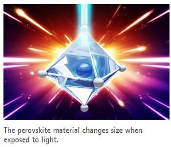
A crystalline material that changes shape in response to light could form the heart of novel light-activated devices. Perovskite crystals have received a lot of attention for their efficiency at converting sunlight into electricity, but new work by scientists at KAUST shows their potential uses extend far beyond the light-harvesting layer of solar panels.
Photostriction is the property of certain materials to undergo a change in internal strain, and therefore shape, with exposure to light. Organic photostrictive materials offer the greatest shape change so far reported in response to light—a parameter known as their photostrictive coefficient—but their response is slow and unstable under ambient conditions.
KAUST electrical engineer Jr-Hau He and his colleagues have looked for photostriction in a new family of materials, the perovskites. “Perovskites are one of the hottest optical materials,” says He. His work now shows there’s more to their interesting optical properties than solar energy harvesting. The researchers tested a perovskite called MAPbBr3 and revealed it had strong and robust photostriction behavior.
To extensively test the material’s photostriction capabilities, the team developed a new method. They used Raman spectroscopy, which probes the molecular vibrations within the structure. When bathed in light, photostriction alters the internal strain in the material, which then shifts the internal pattern of vibrations. By measuring the shift in the Raman signal when the material was placed under mechanical pressure, the team could calibrate the technique and so use it to quantify the effect of photostriction.
“We demonstrated that in situ Raman spectroscopy with confocal microscopy is a powerful characterization tool for conveniently measuring intrinsic photoinduced lattice deformation,” says Tzu-Chiao Wei, a member of the team. “The same approach could be applied to measure photostriction in other materials,” he adds.
The perovskite material proved to have a significant photostriction coefficient of 1.25%. The researchers also showed that the perovskite’s photostriction was partly due to the photovoltaic effect—the phenomenon at the heart of most solar cell operation. The spontaneous generation of positive and negative charges when the perovskite is bathed in light polarizes the material, which induces a movement in the ions the material is made from.
The robust and stable photostriction of perovskite makes it useful for a range of possible devices, says Wei. “We will use this material to fabricate next-generation optoelectronic devices, including wireless remote switchable devices and other light-controlled applications,” he says.
Share on:


Testimonial
"Advertising in PCB007 Magazine has been a great way to showcase our bare board testers to the right audience. The I-Connect007 team makes the process smooth and professional. We’re proud to be featured in such a trusted publication."
Klaus Koziol - atgSuggested Items
September 2025 PCB007 Magazine: The Future of Advanced Materials
09/16/2025 | I-Connect007 Editorial TeamMoore’s Law is no more, and the advanced material solutions being developed to grapple with this reality are surprising, stunning, and perhaps a bit daunting. Buckle up for a dive into advanced materials and a glimpse into the next chapters of electronics manufacturing.
I-Connect007 Launches Advanced Electronics Packaging Digest
09/15/2025 | I-Connect007I-Connect007 is pleased to announce the launch of Advanced Electronics Packaging Digest (AEPD), a new monthly digital newsletter dedicated to one of the most critical and rapidly evolving areas of electronics manufacturing: advanced packaging at the interconnect level.
Panasonic Industry will Double the Production Capacity of MEGTRON Multi-layer Circuit Board Materials Over the Next Five Years
09/15/2025 | Panasonic Industry Co., Ltd.Panasonic Industry Co., Ltd., a Panasonic Group company, announced plans for a major expansion of its global production capacity for MEGTRON multi-layer circuit board materials today. The company plans to double its production over the next five years to meet growing demand in the AI server and ICT infrastructure markets.
Trouble in Your Tank: Implementing Direct Metallization in Advanced Substrate Packaging
09/15/2025 | Michael Carano -- Column: Trouble in Your TankDirect metallization systems based on conductive graphite are gaining popularity throughout the world. The environmental and productivity gains achievable with this process are outstanding. Direct metallization reduces the costs of compliance, waste treatment, and legal issues related to chemical exposure. A graphite-based direct plate system has been devised to address these needs.
Fresh PCB Concepts: Designing for Success at the Rigid-flex Transition Area
08/28/2025 | Team NCAB -- Column: Fresh PCB ConceptsRigid-flex PCBs come in all shapes and sizes. Manufacturers typically use fire-retardant, grade 4 (FR-4) materials in the rigid section and flexible polyimide materials in the flex region. Because of the small size, some rigid-flex PCBs, like those for hearing aid devices, are among the most challenging to manufacture. However, regardless of its size, we should not neglect the transition area between the rigid and flexible material.