


 Trouble in Your Tank: Implementing Direct Metallization in Advanced Substrate Packaging
 It’s Only Common Sense: Storytelling That Sells—Stop Pitching, Start Painting Pictures
 The Right Approach: Get Ready for ISO 9001 Version 6


New Results Reveal High Tunability of 2-D Material
August 28, 2017 | Lawrence Berkeley National LaboratoryEstimated reading time: 5 minutes
Two-dimensional materials are a sort of a rookie phenom in the scientific community. They are atomically thin and can exhibit radically different electronic and light-based properties than their thicker, more conventional forms, so researchers are flocking to this fledgling field to find ways to tap these exotic traits.
Applications for 2-D materials range from microchip components to superthin and flexible solar panels and display screens, among a growing list of possible uses. But because their fundamental structure is inherently tiny, they can be tricky to manufacture and measure, and to match with other materials. So while 2-D materials R&D is on the rise, there are still many unknowns about how to isolate, enhance, and manipulate their most desirable qualities.
Now, a science team at the Department of Energy’s Lawrence Berkeley National Laboratory (Berkeley Lab) has precisely measured some previously obscured properties of moly sulfide, a 2-D semiconducting material also known as molybdenum disulfide or MoS2. The team also revealed a powerful tuning mechanism and an interrelationship between its electronic and optical, or light-related, properties.
To best incorporate such monolayer materials into electronic devices, engineers want to know the “band gap,” which is the minimum energy level it takes to jolt electrons away from the atoms they are coupled to, so that they flow freely through the material as electric current flows through a copper wire. Supplying sufficient energy to the electrons by absorbing light, for example, converts the material into an electrically conducting state.
As reported in the Aug. 25 issue of Physical Review Letters, researchers measured the band gap for a monolayer of moly sulfide, which has proved difficult to accurately predict theoretically, and found it to be about 30 percent higher than expected based on previous experiments. They also quantified how the band gap changes with electron density – a phenomenon known as “band gap renormalization.”
“The most critical significance of this work was in finding the band gap,” said Kaiyuan Yao, a graduate student researcher at Berkeley Lab and the University of California, Berkeley, who served as the lead author of the research paper.
“That provides very important guidance to all of the optoelectronic device engineers. They need to know what the band gap is” in orderly to properly connect the 2-D material with other materials and components in a device, Yao said.
Obtaining the direct band gap measurement is challenged by the so-called “exciton effect” in 2-D materials that is produced by a strong pairing between electrons and electron “holes” – vacant positions around an atom where an electron can exist. The strength of this effect can mask measurements of the band gap.
Nicholas Borys, a project scientist at Berkeley Lab’s Molecular Foundry who also participated in the study, said the study also resolves how to tune optical and electronic properties in a 2-D material.
“The real power of our technique, and an important milestone for the physics community, is to discern between these optical and electronic properties,” Borys said.
The team used several tools at the Molecular Foundry, a facility that is open to the scientific community and specializes in the creation and exploration of nanoscale materials.
The Molecular Foundry technique that researchers adapted for use in studying monolayer moly sulfide, known as photoluminescence excitation (PLE) spectroscopy, promises to bring new applications for the material within reach, such as ultrasensitive biosensors and tinier transistors, and also shows promise for similarly pinpointing and manipulating properties in other 2-D materials, researchers said.
The research team measured both the exciton and band gap signals, and then detangled these separate signals. Scientists observed how light was absorbed by electrons in the moly sulfide sample as they adjusted the density of electrons crammed into the sample by changing the electrical voltage on a layer of charged silicon that sat below the moly sulfide monolayer.
This image shows a slight “bump” (red arrow) in charted experimental data that reveals the band gap measurement in a 2-D material known as moly sulfide. (Credit: Berkeley Lab)
Researchers noticed a slight “bump” in their measurements that they realized was a direct measurement of the band gap, and through a slew of other experiments used their discovery to study how the band gap was readily tunable by simply adjusting the density of electrons in the material.
“The large degree of tunability really opens people’s eyes,” said P. James Schuck, who was director of the Imaging and Manipulation of Nanostructures facility at the Molecular Foundry during this study.
“And because we could see both the band gap’s edge and the excitons simultaneously, we could understand each independently and also understand the relationship between them,” said Schuck, who is now at Columbia University. “It turns out all of these properties are dependent on one another.”
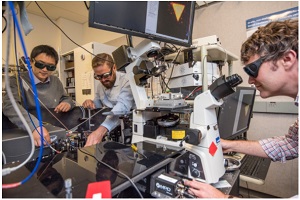
Kaiyuan Yao works with equipment at Berkeley Lab’s Molecular Foundry that was used to help measure a property in a 2-D material. (Credit: Marilyn Chung/Berkeley Lab)
Moly sulfide, Schuck also noted, is “extremely sensitive to its local environment,” which makes it a prime candidate for use in a range of sensors. Because it is highly sensitive to both optical and electronic effects, it could translate incoming light into electronic signals and vice versa.
Schuck said the team hopes to use a suite of techniques at the Molecular Foundry to create other types of monolayer materials and samples of stacked 2-D layers, and to obtain definitive band gap measurements for these, too. “It turns out no one yet knows the band gaps for some of these other materials,” he said.
The team also has expertise in the use of a nanoscale probe to map the electronic behavior across a given sample.
Borys added, “We certainly hope this work seeds further studies on other 2-D semiconductor systems.”
The Molecular Foundry is a DOE Office of Science User Facility that provides free access to state-of-the-art equipment and multidisciplinary expertise in nanoscale science to visiting scientists.
Researchers from the Kavli Energy NanoSciences Institute at UC Berkeley and Berkeley Lab, and from Arizona State University also participated in this study, which was supported by the National Science Foundation.
About Lawrence Berkeley National Laboratory
Lawrence Berkeley National Laboratory addresses the world’s most urgent scientific challenges by advancing sustainable energy, protecting human health, creating new materials, and revealing the origin and fate of the universe. Founded in 1931, Berkeley Lab’s scientific expertise has been recognized with 13 Nobel Prizes. The University of California manages Berkeley Lab for the U.S. Department of Energy’s Office of Science. For more, visit www.lbl.gov.
Share on:


Testimonial
"In a year when every marketing dollar mattered, I chose to keep I-Connect007 in our 2025 plan. Their commitment to high-quality, insightful content aligns with Koh Young’s values and helps readers navigate a changing industry. "
Brent Fischthal - Koh YoungSuggested Items
Trouble in Your Tank: Implementing Direct Metallization in Advanced Substrate Packaging
09/15/2025 | Michael Carano -- Column: Trouble in Your TankDirect metallization systems based on conductive graphite are gaining popularity throughout the world. The environmental and productivity gains achievable with this process are outstanding. Direct metallization reduces the costs of compliance, waste treatment, and legal issues related to chemical exposure. A graphite-based direct plate system has been devised to address these needs.
Closing the Loop on PCB Etching Waste
09/09/2025 | Shawn Stone, IECAs the PCB industry continues its push toward greener, more cost-efficient operations, Sigma Engineering’s Mecer System offers a comprehensive solution to two of the industry’s most persistent pain points: etchant consumption and rinse water waste. Designed as a modular, fully automated platform, the Mecer System regenerates spent copper etchants—both alkaline and acidic—and simultaneously recycles rinse water, transforming a traditionally linear chemical process into a closed-loop system.
Driving Innovation: Depth Routing Processes—Achieving Unparalleled Precision in Complex PCBs
09/08/2025 | Kurt Palmer -- Column: Driving InnovationIn PCB manufacturing, the demand for increasingly complex and miniaturized designs continually pushes the boundaries of traditional fabrication methods, including depth routing. Success in these applications demands not only on robust machinery but also sophisticated control functions. PCB manufacturers rely on advanced machine features and process methodologies to meet their precise depth routing goals. Here, I’ll explore some crucial functions that empower manufacturers to master complex depth routing challenges.
Trouble in Your Tank: Minimizing Small-via Defects for High-reliability PCBs
08/27/2025 | Michael Carano -- Column: Trouble in Your TankTo quote the comedian Stephen Wright, “If at first you don’t succeed, then skydiving is not for you.” That can be the battle cry when you find that only small-diameter vias are exhibiting voids. Why are small holes more prone to voids than larger vias when processed through electroless copper? There are several reasons.
The Government Circuit: Navigating New Trade Headwinds and New Partnerships
08/25/2025 | Chris Mitchell -- Column: The Government CircuitAs global trade winds continue to howl, the electronics manufacturing industry finds itself at a critical juncture. After months of warnings, the U.S. Government has implemented a broad array of tariff increases, with fresh duties hitting copper-based products, semiconductors, and imports from many nations. On the positive side, tentative trade agreements with Europe, China, Japan, and other nations are providing at least some clarity and counterbalance.