


 Trouble in Your Tank: Implementing Direct Metallization in Advanced Substrate Packaging
 It’s Only Common Sense: Storytelling That Sells—Stop Pitching, Start Painting Pictures
 The Right Approach: Get Ready for ISO 9001 Version 6


Nagoya-led Team Flips the Switch on Ferroelectrics
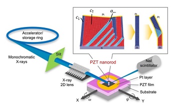
August 29, 2017 | Nagoya UniversityEstimated reading time: 1 minute
Many next-generation electronic and electro-mechanical device technologies hinge on the development of ferroelectric materials. The unusual crystal structures of these materials have regions in their lattice, or domains, that behave like molecular switches. The alignment of a domain can be toggled by an electric field, which changes the position of atoms in the crystal and switches the polarization direction. These crystals are typically grown on supporting substrates that help to define and organize the behavior of domains. Control over the switching of domains when making crystals of ferroelectric materials is essential for any future applications.
Now an international team by Nagoya University has developed a new way of controlling the domain structure of ferroelectric materials, which could accelerate development of future electronic and electro-mechanical devices.
"We grew lead zirconate titanate films on different substrate types to induce different kinds of physical strain, and then selectively etched parts of the films to create nanorods," says lead author Tomoaki Yamada. "The domain structure of the nanorods was almost completely flipped compared with [that of] the thin film."
Lead zirconate titanate is a common type of ferroelectric material, which switches based on the movement of trapped lead atoms between two stable positions in the crystal lattice. Parts of the film were deliberately removed to leave freestanding rods on the substrates. The team then used synchrotron X-ray radiation to probe the domain structure of individual rods.
The contact area of the rods with the substrate was greatly reduced and the domain properties were influenced more by the surrounding environment, which mixed up the domain structure. The team found that coating the rods with a metal could screen the effects of the air and they tended to recover the original domain structure, as determined by the substrate.
"There are few effective ways of manipulating the domain structure of ferroelectric materials, and this becomes more difficult when the material is nanostructured and the contact area with the substrate is small." says collaborator Nava Setter. "We have learned that it's possible to nanostructure these materials with control over their domains, which is an essential step towards the new functional nanoscale devices promised by these materials."
Share on:


Testimonial
"Our marketing partnership with I-Connect007 is already delivering. Just a day after our press release went live, we received a direct inquiry about our updated products!"
Rachael Temple - AlltematedSuggested Items
September 2025 PCB007 Magazine: The Future of Advanced Materials
09/16/2025 | I-Connect007 Editorial TeamMoore’s Law is no more, and the advanced material solutions being developed to grapple with this reality are surprising, stunning, and perhaps a bit daunting. Buckle up for a dive into advanced materials and a glimpse into the next chapters of electronics manufacturing.
I-Connect007 Launches Advanced Electronics Packaging Digest
09/15/2025 | I-Connect007I-Connect007 is pleased to announce the launch of Advanced Electronics Packaging Digest (AEPD), a new monthly digital newsletter dedicated to one of the most critical and rapidly evolving areas of electronics manufacturing: advanced packaging at the interconnect level.
Panasonic Industry will Double the Production Capacity of MEGTRON Multi-layer Circuit Board Materials Over the Next Five Years
09/15/2025 | Panasonic Industry Co., Ltd.Panasonic Industry Co., Ltd., a Panasonic Group company, announced plans for a major expansion of its global production capacity for MEGTRON multi-layer circuit board materials today. The company plans to double its production over the next five years to meet growing demand in the AI server and ICT infrastructure markets.
Trouble in Your Tank: Implementing Direct Metallization in Advanced Substrate Packaging
09/15/2025 | Michael Carano -- Column: Trouble in Your TankDirect metallization systems based on conductive graphite are gaining popularity throughout the world. The environmental and productivity gains achievable with this process are outstanding. Direct metallization reduces the costs of compliance, waste treatment, and legal issues related to chemical exposure. A graphite-based direct plate system has been devised to address these needs.
Fresh PCB Concepts: Designing for Success at the Rigid-flex Transition Area
08/28/2025 | Team NCAB -- Column: Fresh PCB ConceptsRigid-flex PCBs come in all shapes and sizes. Manufacturers typically use fire-retardant, grade 4 (FR-4) materials in the rigid section and flexible polyimide materials in the flex region. Because of the small size, some rigid-flex PCBs, like those for hearing aid devices, are among the most challenging to manufacture. However, regardless of its size, we should not neglect the transition area between the rigid and flexible material.