


 Trouble in Your Tank: Implementing Direct Metallization in Advanced Substrate Packaging
 It’s Only Common Sense: Storytelling That Sells—Stop Pitching, Start Painting Pictures
 The Right Approach: Get Ready for ISO 9001 Version 6


Synthesizing Pure Graphene, a ‘Miracle Material’
September 4, 2017 | University of ConnecticutEstimated reading time: 5 minutes
Formed deep within the earth, stronger than steel, and thinner than a human hair. These comparisons aren’t describing a new super hero. They’re describing graphene, a substance that some experts have called “the most amazing and versatile” known to mankind.
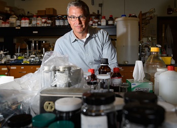
UConn chemistry professor Doug Adamson has found an inexpensive way to manufacture the pristine form of this substance, which is stronger than steel and thinner than a human hair. (Peter Morenus/UConn Photo)
UConn chemistry professor Doug Adamson, a member of the Polymer Program in UConn’s Institute of Materials Science, has patented a one-of-a-kind process for exfoliating this wonder material in its pure (unoxidized) form, as well as manufacturing innovative graphene nanocomposites that have potential uses in a variety of applications.
If you think of graphite like a deck of cards, each individual card would be a sheet of graphene. Comprised of a single layer of carbon atoms arranged in a hexagonal lattice, graphene is a two-dimensional crystal that is at least 100 times stronger than steel. Aerogels made from graphene are some of the lightest materials known to man, and the graphene sheets are one of the thinnest, at only one atom thick – that is approximately one million times thinner than a human hair. Graphene is also even more thermally and electrically conductive than copper, with minimal electrical charge.
Because of these unique qualities, graphene has been a hot topic for academic researchers and industry leaders since it was first isolated from graphite in 2004. Since then, more than 10,000 scholarly articles have been published about the material. But of these publications, only Adamson’s discusses a proprietary process for manufacturing graphene in its pristine form.
What others are calling “graphene” is often actually graphene oxide that has been chemically or thermally reduced. The oxygen in graphene oxide provides a sort of chemical handle that makes the graphene easier to work with, but adding it to pristine graphene reduces the material’s mechanical, thermal, and electrical properties in comparison to unmodified graphene like the kind Adamson produces.
It also significantly increases the cost to manufacture the material. Oxidizing graphite requires adding expensive hazardous chemicals, such as anhydrous sulfuric acid and potassium peroxide, followed by a lengthy series of manipulations to isolate and purify the products, known as a chemistry workup. Adamson’s process doesn’t require any additional steps or chemicals to produce graphene in its pristine form.
“The innovation and technology behind our material is our ability to use a thermodynamically driven approach to un-stack graphite into its constituent graphene sheets, and then arrange those sheets into a continuous, electrically conductive, three-dimensional structure” says Adamson. “The simplicity of our approach is in stark contrast to current techniques used to exfoliate graphite that rely on aggressive oxidation or high-energy mixing or sonication – the application of sound energy to separate particles – for extended periods of time. As straightforward as our process is, no one else had reported it. We proved it works.”
Soon after the initial experiments by graduate student Steve Woltornist indicated that something special was happening, Adamson was joined by longtime collaborator Andrey Dobrynin from the University of Akron, who has helped to understand the thermodynamics that drive the exfoliation. Their work has been published in the American Chemical Society’s peer-reviewed journal ACS Nano.
A distinctive feature of graphene that seems like an obstacle to many – its insolubility – is at the heart of Adamson’s discovery. Since it doesn’t dissolve in liquids, Adamson and his team place graphite at the interface of water and oil, where the graphene sheets spontaneously spread to cover the interface and lower the energy of the system. The graphene sheets are trapped at the interface as individual, overlapping sheets, and can subsequently be locked in place using a cross-linked polymer or plastic.
Adamson began exploring ways to exfoliate graphene from graphite in 2010 with a grant from the Air Force to synthesize thermally conductive composites. This was followed in 2012 with funding from a National Science Foundation (NSF) Early-concept Grants for Exploratory Research (EAGER) award. Since then he has also been awarded a $1.2 million grant from the NSF Designing Materials to Revolutionize and Engineer our Future program and $50,000 from UConn’s SPARK Technology Commercialization Fund program.
“Dr. Adamson’s work speaks not only to the preeminence of UConn’s faculty, but also to the potential real-world applications of their research,” says Radenka Maric, vice president for research at UConn and UConn Health. “The University is committed to programs like SPARK that enable faculty to think about the broader impact of their work and create products or services that will benefit society and the state’s economy.”
Graphene for Water Desalination
While stabilized graphene composite materials have countless potential uses in fields as varied as aircrafts, electronics, and biotechnology, Adamson chose to apply his technology to improving standard methods for the desalination of brackish water. With his SPARK funding, he is developing a device that uses his graphene nanocomposite materials to remove salt from water through a process called capacitive deionization, or CDI.
CDI relies on inexpensive, high surface area, porous electrodes to remove salt from water. There are two cycles in the CDI process: an adsorption phase where the dissolved salt is removed from the water, and a desorption phase where the adsorbed salts are released from the electrodes by either halting or reversing the charge on the electrodes.
Many materials have been used to create the electrodes, but none have proven to be a viable material for large-scale commercialization. Adamson and his industry partners believe that his simple, inexpensive, and robust material could be the technology that finally brings CDI to market in a major way.
“The product we are developing will be an inexpensive graphene material, with optimized performance as an electrode, that will be able to displace more expensive, less efficient materials currently used in CDI,” says Michael Reeve, one of Adamson’s partners and a veteran of various successful startups.
The team formed a startup called 2D Material Technologies, and they have applied for a Small Business Innovation Research grant to continue to commercialize Adamson’s technology. Eventually, they hope to join UConn’s Technology Incubation Program to advance their concept to market.
Share on:


Testimonial
"In a year when every marketing dollar mattered, I chose to keep I-Connect007 in our 2025 plan. Their commitment to high-quality, insightful content aligns with Koh Young’s values and helps readers navigate a changing industry. "
Brent Fischthal - Koh YoungSuggested Items
Trouble in Your Tank: Implementing Direct Metallization in Advanced Substrate Packaging
09/15/2025 | Michael Carano -- Column: Trouble in Your TankDirect metallization systems based on conductive graphite are gaining popularity throughout the world. The environmental and productivity gains achievable with this process are outstanding. Direct metallization reduces the costs of compliance, waste treatment, and legal issues related to chemical exposure. A graphite-based direct plate system has been devised to address these needs.
Closing the Loop on PCB Etching Waste
09/09/2025 | Shawn Stone, IECAs the PCB industry continues its push toward greener, more cost-efficient operations, Sigma Engineering’s Mecer System offers a comprehensive solution to two of the industry’s most persistent pain points: etchant consumption and rinse water waste. Designed as a modular, fully automated platform, the Mecer System regenerates spent copper etchants—both alkaline and acidic—and simultaneously recycles rinse water, transforming a traditionally linear chemical process into a closed-loop system.
Driving Innovation: Depth Routing Processes—Achieving Unparalleled Precision in Complex PCBs
09/08/2025 | Kurt Palmer -- Column: Driving InnovationIn PCB manufacturing, the demand for increasingly complex and miniaturized designs continually pushes the boundaries of traditional fabrication methods, including depth routing. Success in these applications demands not only on robust machinery but also sophisticated control functions. PCB manufacturers rely on advanced machine features and process methodologies to meet their precise depth routing goals. Here, I’ll explore some crucial functions that empower manufacturers to master complex depth routing challenges.
Trouble in Your Tank: Minimizing Small-via Defects for High-reliability PCBs
08/27/2025 | Michael Carano -- Column: Trouble in Your TankTo quote the comedian Stephen Wright, “If at first you don’t succeed, then skydiving is not for you.” That can be the battle cry when you find that only small-diameter vias are exhibiting voids. Why are small holes more prone to voids than larger vias when processed through electroless copper? There are several reasons.
The Government Circuit: Navigating New Trade Headwinds and New Partnerships
08/25/2025 | Chris Mitchell -- Column: The Government CircuitAs global trade winds continue to howl, the electronics manufacturing industry finds itself at a critical juncture. After months of warnings, the U.S. Government has implemented a broad array of tariff increases, with fresh duties hitting copper-based products, semiconductors, and imports from many nations. On the positive side, tentative trade agreements with Europe, China, Japan, and other nations are providing at least some clarity and counterbalance.