


 Trouble in Your Tank: Implementing Direct Metallization in Advanced Substrate Packaging
 It’s Only Common Sense: Storytelling That Sells—Stop Pitching, Start Painting Pictures
 The Right Approach: Get Ready for ISO 9001 Version 6


Carving Diamonds for Optical Components
September 5, 2017 | EPFLEstimated reading time: 2 minutes
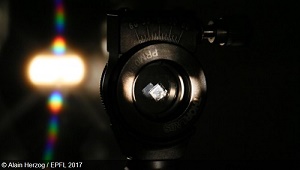
Thanks to a new technique developed at EPFL, optical diffraction gratings can now be made out of pure diamond, with their surfaces smoothed down to the very last atom. These new devices can be used to alter the wavelength of high-powered lasers or in cutting-edge spectrographs.
A team of EPFL researchers has developed an unconventional way of microscopically cutting diamonds into a particular shape and smoothing them at an atomic level. This new technique, which will be presented at the International Conference on Diamond and Carbon Materials DCM2017 on 5 September, makes it possible to manufacture diffraction gratings out of pure diamond, which has unique properties that are ideal for both spectroscopy and the optical components used in high-powered lasers.
Diffraction gratings are made up of parallel grooves that break up light into its spectral components, kind of like a prism. These gratings are usually made out of glass and silicon, materials that have already been used in spectrographs and to alter the color emitted by lasers.
The team, led by Niels Quack, a SNSF-funded professor at the School of Engineering, has now found a way to make these gratings out of single crystal diamond as well, opening up the field to an array of new possibilities. Diamonds are unmatched in terms of their thermal conductivity, which is between five and ten times greater than that of any other material used for this purpose. Diamonds are also extremely hard and work well with UV rays, as well as infrared and visible beams. "Diamonds are chemically inert, which means that even the most aggressive chemical substances can't attack them. But it also means that they are very difficult to machine," explains Dr. Quack. "So this new way of carving diamonds could prove very useful."
Using oxygen to cut diamonds
The technique developed by the researchers is groundbreaking because it allows them to etch well defined shapes into millimeter sized single-crystal diamond plates, with the grooves separated by just a few microns and with incredibly smooth surfaces. To develop their technique, the researchers used diamonds created synthetically through chemical vapor deposition.
The diamonds are etched in several stages. First, a hard mask is deposited and structured on the surface of a diamond plate, which is then exposed to an oxygen plasma. The oxygen ions in the plasma are accelerated onto the surface of the diamond by an electric field. Where not covered by the hard mask, the oxygen ions remove carbon atoms from the diamond’s surface one by one. "By adjusting the intensity of the electric field, we can alter the shape we etch into the diamond," explains Dr. Quack. "For the diffraction gratings, we carve out triangular grooves that are just a few microns apart from each other. We adjust the process parameters to selectively reveal a set of well-defined crystal planes, allowing us to create V-shaped grooves that are smoothed down almost to the atomic level. It is impossible to get this kind of precision when the diamonds are simply cut with a laser."
This new technology, which was developed using the facilities in the Center of MicroNanoTechnology (CMI), is the subject of a recent patent application. The same principle has already been used using silicon, but it had never before been demonstrated in diamond. In recognition of the importance of this contribution, doctoral student Marcell Kiss has been shortlisted as one of the six finalists of the Young Scholar Award DCM2017.
Share on:


Testimonial
"We’re proud to call I-Connect007 a trusted partner. Their innovative approach and industry insight made our podcast collaboration a success by connecting us with the right audience and delivering real results."
Julia McCaffrey - NCAB GroupSuggested Items
Electra’s ElectraJet EMJ110 Inkjet Soldermask Now in Black & Blue at Sunrise Electronics
09/08/2025 | Electra Polymers LtdFollowing the successful deployment of Electra’s Green EMJ110 Inkjet Soldermask on KLA’s Orbotech Neos™ platform at Sunrise Electronics in Elk Grove Village, Illinois, production has now moved beyond green.
Magnachip Semiconductor Announces YJ Kim to Step Down as CEO; Current Board Chairman Camillo Martino Appointed Interim CEO
08/14/2025 | PR NewswireMagnachip Semiconductor Corporation today announced that YJ Kim has agreed to step down as CEO and as a member of the Board of Directors, effective immediately. Camillo Martino, Chairman of the Board of Directors, has also been appointed Interim Chief Executive Officer, effective immediately.
Bell to Build X-Plane for Phase 2 of DARPA Speed and Runway Independent Technologies (SPRINT) X-Plane Program
07/09/2025 | Bell Textron Inc.Bell Textron Inc., a Textron Inc. company, has been down-selected for Phase 2 of Defense Advanced Research Projects Agency (DARPA) Speed and Runway Independent Technologies (SPRINT) X-Plane program with the objective to complete design, construction, ground testing and certification of an X-plane demonstrator.
Nolan’s Notes: Moving Forward With Confidence
06/03/2025 | Nolan Johnson -- Column: Nolan's NotesWe’re currently enjoying a revitalized and dynamic EMS provider market with significant growth potential. Since December 2024, the book-to-bill has been extremely strong and growing. Starting with a ratio of 1.24 in December, book-to-bill has continued to accelerate to a 1.41 in April. Yet, there is a global economic restructuring taking place. To say that the back-and-forth with tariffs and trade deals makes for an uncertain market is an understatement. While we may be in a 90-day tariff pause among leading economic nations, the deadline is quickly approaching and that leaves many of you feeling unsettled about what to expect.
Mycronic High Flex Changes Division Name to PCB Assembly Solutions
05/20/2025 | MycronicMycronic AB, the leading Sweden-based electronics assembly solutions provider, announced that its division formerly known as High Flex will now operate under the name PCB Assembly Solutions.