


 Trouble in Your Tank: Implementing Direct Metallization in Advanced Substrate Packaging
 It’s Only Common Sense: Storytelling That Sells—Stop Pitching, Start Painting Pictures
 The Right Approach: Get Ready for ISO 9001 Version 6


Supercharging Silicon Batteries
September 6, 2017 | OISTEstimated reading time: 3 minutes
As the world shifts towards renewable energy, moving on from fossil fuels, but at the same time relying on ever more energy-gobbling devices, there is a fast-growing need for larger high-performance batteries. Lithium-ion batteries (LIBs) power most of our portable electronics, but they are flammable and can even explode, as it happened to a recent model of smartphone. To prevent such accidents, the current solution is to encapsulate the anode – which is the negative (-) electrode of the battery, opposite to the cathode (+) - into a graphite frame, thus insulating the lithium ions. However, such casing is limited to a small scale to avoid physical collapse, therefore restraining the capacity - the amount of energy you can store - of the battery.
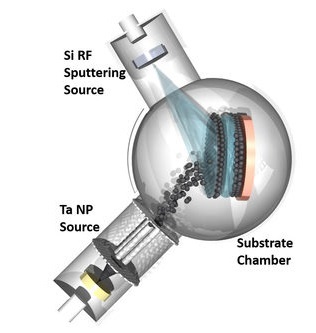
Starting from a copper frame (in orange on the right), the anode is built layer by layer by alternatively depositing Silicon (top) and nanostructured tantalum metal (bottom) with great control. (Photo credit: OIST Nanoparticles by Design Unit)
Looking for better materials, silicon offers great advantages over carbon graphite for lithium batteries in terms of capacity. Six atoms of carbon are required to bind a single atom of lithium, but an atom of silicon can bind four atoms of lithium at the same time, multiplying the battery capacity by more than 10-fold. However, being able to capture that many lithium ions means that the volume of the anode swells by 300% to 400%, leading to fracturing and loss of structural integrity. To overcome this issue, OIST researchers have now reported in Advanced Science the design of an anode built on nanostructured layers of silicon – not unlike a multi-layered cake – to preserve the advantages of silicon while preventing physical collapse.
This new battery is also aiming to improve power, which is the ability to charge and deliver energy over time.
“The goal in battery technology right now is to increase charging speed and power output,” explained Dr. Marta Haro Remon, first author of the study. “While it is fine to charge your phone or your laptop over a long period of time, you would not wait by your electric car for three hours at the charging station.”
And when it comes to providing energy, you would want your car to start off quickly at a traffic light or a stop sign, requiring a high spike in power, rather than slowly creeping forward. A well-thought design of a silicone-based anode might be a solution and answer these expectations.
The idea behind the new anode in the Nanoparticles by Design Unit at the Okinawa Institute of Science and Technology Graduate University is the ability to precisely control the synthesis and the corresponding physical structure of the nanoparticles. Layers of unstructured silicon films are deposited alternatively with tantalum metal nanoparticle scaffolds, resulting in the silicon being sandwiched in a tantalum frame.
“We used a technique called Cluster Beam Deposition,” continued Dr. Haro. “The required materials are directly deposited on the surface with great control. This is a purely physical method, there are no need for chemicals, catalysts or other binders.”
“We used a technique called Cluster Beam Deposition,” continued Dr. Haro. “The required materials are directly deposited on the surface with great control. This is a purely physical method, there are no need for chemicals, catalysts or other binders.”
The outcome of this research, led by Prof. Sowwan at OIST, is an anode with higher power but restrained swelling, and excellent cyclability – the amount of cycles in which a battery can be charged and discharged before losing efficiency. By looking closer into the nanostructured layers of silicon, the scientists realized the silicon shows important porosity with a grain-like structure in which lithium ions could travel at higher speeds compared to unstructured, amorphous silicon, explaining the increase in power. At the same time the presence of silicon channels along the Ta nanoparticle scaffolds allows the lithium ions to diffuse in the entire structure. On the other hand, the tantalum metal casing, while restraining swelling and improving structural integrity, also limited the overall capacity – for now.
However, this design is currently only at the stage of proof-of-concept, opening the door to numerous opportunities to improve capacity along with the increased power.
“It is a very open synthesis approach, there are many parameters you can play around,” commented Dr. Haro. “For example, we want to optimize the numbers of layers, their thickness, and replace tantalum metal with other materials.”
With this technique paving the way, it might very well be that the solution for future batteries, forecast to be omnipresent in our lives, will be found in nanoparticles.
Original by: Wilko Duprez
Share on:


Testimonial
"The I-Connect007 team is outstanding—kind, responsive, and a true marketing partner. Their design team created fresh, eye-catching ads, and their editorial support polished our content to let our brand shine. Thank you all! "
Sweeney Ng - CEE PCBSuggested Items
Trouble in Your Tank: Implementing Direct Metallization in Advanced Substrate Packaging
09/15/2025 | Michael Carano -- Column: Trouble in Your TankDirect metallization systems based on conductive graphite are gaining popularity throughout the world. The environmental and productivity gains achievable with this process are outstanding. Direct metallization reduces the costs of compliance, waste treatment, and legal issues related to chemical exposure. A graphite-based direct plate system has been devised to address these needs.
Closing the Loop on PCB Etching Waste
09/09/2025 | Shawn Stone, IECAs the PCB industry continues its push toward greener, more cost-efficient operations, Sigma Engineering’s Mecer System offers a comprehensive solution to two of the industry’s most persistent pain points: etchant consumption and rinse water waste. Designed as a modular, fully automated platform, the Mecer System regenerates spent copper etchants—both alkaline and acidic—and simultaneously recycles rinse water, transforming a traditionally linear chemical process into a closed-loop system.
Driving Innovation: Depth Routing Processes—Achieving Unparalleled Precision in Complex PCBs
09/08/2025 | Kurt Palmer -- Column: Driving InnovationIn PCB manufacturing, the demand for increasingly complex and miniaturized designs continually pushes the boundaries of traditional fabrication methods, including depth routing. Success in these applications demands not only on robust machinery but also sophisticated control functions. PCB manufacturers rely on advanced machine features and process methodologies to meet their precise depth routing goals. Here, I’ll explore some crucial functions that empower manufacturers to master complex depth routing challenges.
Trouble in Your Tank: Minimizing Small-via Defects for High-reliability PCBs
08/27/2025 | Michael Carano -- Column: Trouble in Your TankTo quote the comedian Stephen Wright, “If at first you don’t succeed, then skydiving is not for you.” That can be the battle cry when you find that only small-diameter vias are exhibiting voids. Why are small holes more prone to voids than larger vias when processed through electroless copper? There are several reasons.
The Government Circuit: Navigating New Trade Headwinds and New Partnerships
08/25/2025 | Chris Mitchell -- Column: The Government CircuitAs global trade winds continue to howl, the electronics manufacturing industry finds itself at a critical juncture. After months of warnings, the U.S. Government has implemented a broad array of tariff increases, with fresh duties hitting copper-based products, semiconductors, and imports from many nations. On the positive side, tentative trade agreements with Europe, China, Japan, and other nations are providing at least some clarity and counterbalance.