


 Trouble in Your Tank: Implementing Direct Metallization in Advanced Substrate Packaging
 It’s Only Common Sense: Storytelling That Sells—Stop Pitching, Start Painting Pictures
 The Right Approach: Get Ready for ISO 9001 Version 6


Newly Discovered Semiconductor Dynamics May Help Improve Energy Efficiency
September 6, 2017 | UICEstimated reading time: 2 minutes
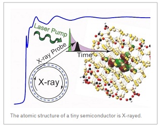
Researchers examining the flow of electricity through semiconductors have uncovered another reason these materials seem to lose their ability to carry a charge as they become more densely “doped.”
Semiconductors are found in just about every piece of modern electronics, from computers to televisions to your cell phone. They fall somewhere between metals, which conduct electricity very well, and insulators like glass that don’t conduct electricity at all. This moderate conduction property is what allows semiconductors to perform as switches and transistors in electronics.
The most common material for semiconductors is silicon, which is mined from the earth and then refined and purified. But pure silicon doesn’t conduct electricity, so the material is purposely and precisely adulterated by the addition of other substances known as dopants. Boron and phosphorus ions are common dopants added to silicon-based semiconductors that allow them to conduct electricity.
But the amount of dopant added to a semiconductor matters – too little dopant and the semiconductor won’t be able to conduct electricity. Too much dopant and the semiconductor becomes more like a non-conductive insulator.
“There’s a sweet spot when it comes to doping where the right amount allows for the efficient conduction of electricity, but after a certain point, adding more dopants slows down the flow,” says Preston Snee, associate professor of chemistry at the University of Illinois at Chicago and corresponding author on the paper.
“For a long time scientists thought that the reason efficient conduction of electricity dropped off with the addition of more dopants was because these dopants caused the flowing electrons to be deflected away, but we found that there’s also another way too many dopants impede the flow of electricity.”
Snee, UIC chemistry student Asra Hassan, and their colleagues wanted to get a closer look at what happens when electricity flows through a semiconductor.
Using the Advanced Photon Source Argonne National Laboratory, they were able to capture X-ray images of what happens at the atomic level inside a semiconductor. They used tiny chips of cadmium sulfide for their semiconductor “base” and doped them with copper ions. Instead of wiring the tiny chips for electricity, they generated a flow of electrons through the semiconductors by shooting them with a powerful blue laser beam. At the same time, they took very high energy X-ray photos of the semiconductors at millionths of a microsecond apart – which showed what was happening at the atomic level in real time as electrons flowed through the doped semiconductors.
They found that when electrons were flowing through, the copper ions transiently formed bonds with the cadmium sulfate semiconductor base, which is detrimental to conduction.
“This has never been seen before,” said Hassan. “Electrons are still bouncing off dopants, which we knew already, but we now know of this other process that contributes to impeding flow of electricity in over-doped semiconductors.”
The bonding of the dopant ions to the semiconductor base material “causes the current to get stuck at the dopants, which we don’t want in our electronics, especially if we want them to be fast and efficient,” she said. “However, now that we know this is happening inside the material, we can design smarter systems that minimize this effect, which we call ‘charge carrier modulation of dopant bonding’.”
Xiaohan Liu, Ali Jawaid, Ahmet Gulec, Robert Klie and Armen Shamirian of UIC; Xiaoyi Zhang, Soma Chattopadhyay, Xiaobing Zuo of Argonne National Laboratory and Clare Rowland and Richard Schaller of Northwestern University are co-authors on the paper.
Share on:


Testimonial
"Our marketing partnership with I-Connect007 is already delivering. Just a day after our press release went live, we received a direct inquiry about our updated products!"
Rachael Temple - AlltematedSuggested Items
Trouble in Your Tank: Implementing Direct Metallization in Advanced Substrate Packaging
09/15/2025 | Michael Carano -- Column: Trouble in Your TankDirect metallization systems based on conductive graphite are gaining popularity throughout the world. The environmental and productivity gains achievable with this process are outstanding. Direct metallization reduces the costs of compliance, waste treatment, and legal issues related to chemical exposure. A graphite-based direct plate system has been devised to address these needs.
Closing the Loop on PCB Etching Waste
09/09/2025 | Shawn Stone, IECAs the PCB industry continues its push toward greener, more cost-efficient operations, Sigma Engineering’s Mecer System offers a comprehensive solution to two of the industry’s most persistent pain points: etchant consumption and rinse water waste. Designed as a modular, fully automated platform, the Mecer System regenerates spent copper etchants—both alkaline and acidic—and simultaneously recycles rinse water, transforming a traditionally linear chemical process into a closed-loop system.
Driving Innovation: Depth Routing Processes—Achieving Unparalleled Precision in Complex PCBs
09/08/2025 | Kurt Palmer -- Column: Driving InnovationIn PCB manufacturing, the demand for increasingly complex and miniaturized designs continually pushes the boundaries of traditional fabrication methods, including depth routing. Success in these applications demands not only on robust machinery but also sophisticated control functions. PCB manufacturers rely on advanced machine features and process methodologies to meet their precise depth routing goals. Here, I’ll explore some crucial functions that empower manufacturers to master complex depth routing challenges.
Trouble in Your Tank: Minimizing Small-via Defects for High-reliability PCBs
08/27/2025 | Michael Carano -- Column: Trouble in Your TankTo quote the comedian Stephen Wright, “If at first you don’t succeed, then skydiving is not for you.” That can be the battle cry when you find that only small-diameter vias are exhibiting voids. Why are small holes more prone to voids than larger vias when processed through electroless copper? There are several reasons.
The Government Circuit: Navigating New Trade Headwinds and New Partnerships
08/25/2025 | Chris Mitchell -- Column: The Government CircuitAs global trade winds continue to howl, the electronics manufacturing industry finds itself at a critical juncture. After months of warnings, the U.S. Government has implemented a broad array of tariff increases, with fresh duties hitting copper-based products, semiconductors, and imports from many nations. On the positive side, tentative trade agreements with Europe, China, Japan, and other nations are providing at least some clarity and counterbalance.