


 Global PCB Connections: Rigid-flex and Flexible PCBs—The Backbone of Modern Electronics
 Flexible Thinking: The Key to a Successful Flex Circuit Design Transfer
 Happy’s Tech Talk #29: Bend-to-Install Semi-flex FR-4


A New Way to Print Electrical Circuits
September 7, 2017 | Northwestern UniversityEstimated reading time: 3 minutes
Within 15 minutes of meeting Mark Hersam, PhD, a renowned nanotechnology expert and professor of materials science and engineering at Northwestern University, Ethan Secor knew he wanted to work with him. Secor, a fifth year materials science and engineering PhD candidate, didn’t have a project in mind at the time, but when Hersam had an opening in his research group, he jumped right in — and hasn’t looked back.
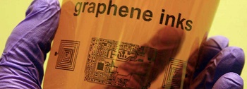
Secor, from Stillwater, Minnesota, is developing graphene-based inks, which can be printed with traditional methods like inkjet printing. With the thickness of an atom, graphene is the thinnest material in the world — and one of its greatest potentials is its ability to be used as a conductor.
“For printed electronics, instead of printing red, green and blue inks, we’re printing conductors, semiconductors and insulators — different classes of electronically functional materials,” says Secor. “So instead of printing pictures, we’re printing electronic circuits.”
Scaling up
With this project’s potential for large-scale impact, Secor says there are more questions than they have time to address — and Hersam’s ability to identify the ones to answer is invaluable.
“From the beginning, Professor Hersam was very optimistic about the overall project,” said Secor. “He provided the necessary impetus to target bottlenecks in order to increase our capabilities in the lab.”
For example, when Secor started, he was making 100 milligrams of graphene at a time — which was time-consuming. Hersam encouraged Secor to explore different ways to improve the process, even investing in expanded lab capabilities so Secor could make graphene one gram at a time. “That allowed us to do considerably more — we could supply the material to collaborators and we could go after projects that wouldn’t otherwise be possible,” says Secor.
The payoff
Printing electronics with graphene inks — either on paper or plastic substrates — not only reduces the manufacturing costs of electronic components, but it also allows the use of flexible surfaces. This is critical to integrating electronics into clothing, consumer electronics and products.
“Instead of depositing the material we want everywhere and selectively removing it where we don’t — how electronics are typically manufactured — we’re only putting material where it’s needed, so there’s less waste,” says Secor. “We’re taking mature, high-speed printing methods designed to print out hundreds of thousands of magazines and applying them to electronics.” For example, if you want to cover the desert in solar panels, it doesn’t make sense to use the technology used to fabricate computer chips. Printed electronics allow you to scale larger — even to square meters and beyond — very easily.
One reason Secor is passionate about this project is that, unlike some research projects, the practical value of graphene inks will impact everyday consumers in the very near future in a number of ways:
- Displays: Lightweight, flexible TV or computer monitors that will be portable.
- Smart packaging: Sensors integrated into food packaging that can detect and signal when a product is going bad to reduce food waste.
- Wearable devices: Improved smart watch and fitness monitor design could integrate their tracking capabilities into clothing for more accurate monitoring of the body’s performance, temperature, pulse and hydration.
Since graphene offers an agile, low-cost platform, printed electronics can also open up opportunities for smaller companies to get into the industry — leading to a more innovative, dynamic market.
Inspiring future groundbreakers
Secor is just one of 30 PhD students Hersam has worked with in his research group at Northwestern — and beyond his group, that number is even higher. Throughout the science and engineering departments, Hersam’s dedication to educating the next generation of scientists is something he is known for. “The impact of a university is made by its students,” says Hersam. “The beauty of a field like nanotechnology is that it captures the imagination of young people, and will continue attracting them and bringing in the best talent.”
Hersam says he and his colleagues work hard to inspire as many students as they can. “The combined outcome of our graduate students will exceed our own,” he says. “And for nanotechnology — an area of science that truly has no limits — that’s fantastic for all society.”
Share on:


Testimonial
"In a year when every marketing dollar mattered, I chose to keep I-Connect007 in our 2025 plan. Their commitment to high-quality, insightful content aligns with Koh Young’s values and helps readers navigate a changing industry. "
Brent Fischthal - Koh YoungSuggested Items
Smartphone Production Rises 4% QoQ in 2Q25 as Inventory Adjustment Ends
09/12/2025 | TrendForceTrendForce’s latest investigations reveal that global smartphone production reached 300 million units in 2Q25, up 4% QoQ and 4.8% YoY, driven by seasonal demand and the recovery of brands such as Oppo and Transsion following inventory adjustments.
I-Connect007 Editor’s Choice: Five Must-Reads for the Week
09/12/2025 | Marcy LaRont, I-Connect007We may be post-Labor Day, but it is still hot-hot-hot here in the great state of Arizona—much like our news cycles, which have continued to snap, crackle, and pop with eye-raising headlines over this past week. In broader global tech news this week, AI and tariff-type restrictions continues to dominate with NVIDIA raising its voice against U.S. lawmakers pushing chip restrictions, ASML investing in a Dutch AI start-up company to the tune of $1.5 billion, and the UAE joining the ranks of the U.S. and China in embracing “open source” with their technology in hopes of accelerating their AI position.
Delta Electronics Posts 26.7% Growth in Sales Revenues for August
09/12/2025 | Delta ElectronicsDelta Electronics, Inc. announced its consolidated sales revenues for August 2025 totaled NT$47,860 million, a 26.7 percent increase as compared to NT$37,770 million for August 2024 and a 5.4 percent increase as compared to NT$45,397 million for July 2025.
Flex Named to TIME's World's Best Companies List for Third Consecutive Year
09/12/2025 | FlexFlex announced its inclusion on the TIME World's Best Companies 2025 list. This marks the third consecutive year the company was included in this prestigious ranking, which recognizes top-performing companies across the globe.
Direct Imaging System Market Size to Hit $4.30B by 2032, Driven by Increasing Demand for High-Precision PCB Manufacturing
09/11/2025 | Globe NewswireAccording to the SNS Insider, “The Direct Imaging System Market size was valued at $2.21 Billion in 2024 and is projected to reach $4.30 Billion by 2032, growing at a CAGR of 8.68% during 2025-2032.”