


 Global PCB Connections: Rigid-flex and Flexible PCBs—The Backbone of Modern Electronics
 Flexible Thinking: The Key to a Successful Flex Circuit Design Transfer
 Happy’s Tech Talk #29: Bend-to-Install Semi-flex FR-4


Graphene-based Terahertz Absorbers
September 12, 2017 | Graphene FlagshipEstimated reading time: 2 minutes
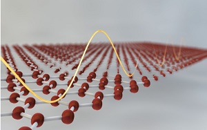
Graphene Flagship researches from CNR-Istituto Nanoscienze, Italy and the University of Cambridge, UK have shown that it is possible to create a terahertz saturable absorber using graphene produced by liquid phase exfoliation and deposited by transfer coating and ink jet printing.
A terahertz saturable absorber decreases its absorption of light in the terahertz range (far infrared) with increasing light intensity and has great potential for the development of terahertz lasers, with applications in spectroscopy and imaging. These high-modulation, mode-locked lasers open up many prospects in applications where short time scale excitation of specific transitions are important, such as time-resolved spectroscopy of gasses and molecules, quantum information or ultra-high speed communication.
“We started working on saturable terahertz absorbers to solve the problem of producing a miniaturized mode-locked terahertz laser with thin and flexible integrated components that also had good modulation” said Graphene Flagship researcher Miriam Vitiello from CNR-Istituto Nanoscienze in Italy.
Graphene is a promising saturable absorber as it has intrinsic broadband operations and ultrafast recovery time along with an ease of fabrication and integration, as first demonstrated in ultra-fast infra-red lasers by Flagship partner University of Cambridge. In the terahertz range, the present paper exploits graphene produced by liquid phase exfoliation, a method ideally suited to mass production, to prepare inks, easily deposited by transfer coating or ink jet printing.
“It was important to us to use a type of graphene that could be integrated into the laser system with flexibility and control” said Vitiello “Ink jet printing along with transfer coating achieved that.”
Using mode-locked lasers to produce ultra fast pulses in the terahertz range can have interesting and exciting uses. “These devices could have applications in medical diagnostics when time of flight topography is of importance – you could see a tumour inside a tissue” said Vitiello.
Frank Koppens, of the Institute of Photonic Sciences in Spain, is the leader of the Graphene Flagship’s Photonics and Optoelectronics Work Package, which focuses on developing graphene-based technologies for imaging and sensing, data transfer and other photonics applications. “This is a new discovery with immediate impact on applications. Clearly, this is a case where graphene beats existing materials in terms of efficiency, scalability, compactness and speed” he said.
Andrea C. Ferrari, Science and Technology Officer of the Graphene Flagship, and Chair of its Management Panel added "It is an important milestone to have demonstrated that easily produced and printable graphene inks can also serve to enable ultrafast lasers in the terahertz range. Since the Flagship’s inception, a variety of lasers have been made covering the visible to IR spectral range, but now the important THz range, with applications in security and medical diagnostic, is finally made accessible by graphene, starting yet another possible application field."
Original by: Sian Fogden
Share on:


Testimonial
"Our marketing partnership with I-Connect007 is already delivering. Just a day after our press release went live, we received a direct inquiry about our updated products!"
Rachael Temple - AlltematedSuggested Items
MEMS & Imaging Sensors Summit to Spotlight Sensing Revolution for Europe’s Leadership
09/11/2025 | SEMIIndustry experts will gather November 19-20 at the SEMI MEMS & Imaging Sensors Summit 2025 to explore the latest breakthroughs in AI-driven MEMS and imaging optimization, AR/VR technologies, and advanced sensor solutions for critical defence applications.
Direct Imaging System Market Size to Hit $4.30B by 2032, Driven by Increasing Demand for High-Precision PCB Manufacturing
09/11/2025 | Globe NewswireAccording to the SNS Insider, “The Direct Imaging System Market size was valued at $2.21 Billion in 2024 and is projected to reach $4.30 Billion by 2032, growing at a CAGR of 8.68% during 2025-2032.”
I-Connect007’s Editor’s Choice: Five Must-Reads for the Week
07/04/2025 | Marcy LaRont, I-Connect007For our industry, we have seen several bullish market announcements over the past few weeks, including one this week by IDC on the massive growth in the global server market. We’re also closely watching global trade and nearshoring. One good example of successful nearshoring is Rehm Thermal Systems, which celebrates its 10th anniversary in Mexico and the official opening of its new building in Guadalajara.
Driving Innovation: Direct Imaging vs. Conventional Exposure
07/01/2025 | Simon Khesin -- Column: Driving InnovationMy first camera used Kodak film. I even experimented with developing photos in the bathroom, though I usually dropped the film off at a Kodak center and received the prints two weeks later, only to discover that some images were out of focus or poorly framed. Today, every smartphone contains a high-quality camera capable of producing stunning images instantly.
United Electronics Corporation Advances Manufacturing Capabilities with Schmoll MDI-ST Imaging Equipment
06/24/2025 | United Electronics CorporationUnited Electronics Corporation has successfully installed the advanced Schmoll MDI-ST (XL) imaging equipment at their advanced printed circuit board facility. This significant technology investment represents a continued commitment to delivering superior products and maintaining their position as an industry leader in precision PCB manufacturing.