


 Trouble in Your Tank: Implementing Direct Metallization in Advanced Substrate Packaging
 It’s Only Common Sense: Storytelling That Sells—Stop Pitching, Start Painting Pictures
 The Right Approach: Get Ready for ISO 9001 Version 6


Digging Sensors out of an Efficiency Hole
September 20, 2017 | A*STAREstimated reading time: 2 minutes
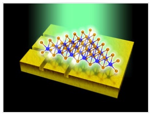
Future ultrathin solar cells and light sources could have their surfaces covered by tiny trenches, after A*STAR researchers found such structures enhance efficiency by four orders of magnitude.
Joel Yang from the A*STAR Institute of Materials Research and Engineering was part of an international collaboration that achieved a 20,000-fold increase in the photoluminescence of a one atom-thick layer of tungsten diselenide, by mounting it on a gold surface patterned with narrow trenches.
Tungsten diselenide is promising for ultra-sensitive, ultra-thin light sensors, solar cells and light-emitting diodes, because of its ability to absorb light and re-emit at a different frequency. However this effect only occurs for a single atom layer, so its efficiency is very low – most of the light passes straight through.
Yang’s inspiration was to mount the layer on a gold surface and trap the light energy at the interface of the two layers in the form of surface plasmons. To enhance the absorption of light, they added trenches to the gold layer under the tungsten diselenide.
“It was very surprising that such a large enhancement could be possible,” says Yang.
The key was matching the trench size to the energy so that the plasmons were trapped in the trenches through a resonant process known as the Purcell effect.
The team shone 633-nanometer light onto the sample and measured the output at 750 nanometers. They found 12 nm wide trenches in a grid pattern with spacing 200 nanometers gave the highest photoluminescence – 20,000 times more than a bare layer of tungsten diselenide.
To create the structure, the team etched a very flat silicon crystal to create a grid of ridges. Next they deposited a layer of gold onto the silicon and then peeled it off to reveal trenches where the ridges had been.
“The narrowness of the trenches and the flatness of the metal film is important,” Yang says. “Any roughness will interact detrimentally with the two-dimensional material.”
The gold was immersed in water and a film of tungsten diselenide floated on the water’s surface. The gold was then slowly raised out of the solution, emerging with the thin layer on top.
The simple structure has many advantages, says Yang. “The entire surface is exposed to the user, which makes it easy for further research, such as functionalizing the surface with chemicals or adding electrodes”.
It is also easier to manufacture than other plasmonic devices, which require a second layer above the thin layer, creating a sandwich.
Share on:


Testimonial
"In a year when every marketing dollar mattered, I chose to keep I-Connect007 in our 2025 plan. Their commitment to high-quality, insightful content aligns with Koh Young’s values and helps readers navigate a changing industry. "
Brent Fischthal - Koh YoungSuggested Items
Driving Innovation: Depth Routing Processes—Achieving Unparalleled Precision in Complex PCBs
09/08/2025 | Kurt Palmer -- Column: Driving InnovationIn PCB manufacturing, the demand for increasingly complex and miniaturized designs continually pushes the boundaries of traditional fabrication methods, including depth routing. Success in these applications demands not only on robust machinery but also sophisticated control functions. PCB manufacturers rely on advanced machine features and process methodologies to meet their precise depth routing goals. Here, I’ll explore some crucial functions that empower manufacturers to master complex depth routing challenges.
Polar Instruments Announces Additive Transmission Line Support for Si9000e
08/20/2025 | Polar InstrumentsTransmission lines embedded into the PCB surface are a feature of UHDI constructions. The 2025 fall release of Polar's Si9000e PCB impedance & insertion loss transmission line field solver incorporates eight new single ended, differential and coplanar transmission line structures.
Henniker Plasma Launches Stratus Turnkey Plasma Manufacturing Cell
08/13/2025 | Henniker PlasmaHenniker Plasma, a leading manufacturer of plasma treatment systems, proudly announces the launch of its Stratus Plasma Manufacturing Cell range — a fully integrated, turnkey solution that combines advanced atmospheric plasma surface treatment with robotic automation.
Trouble in Your Tank: Metallizing Flexible Circuit Materials—Mitigating Deposit Stress
08/04/2025 | Michael Carano -- Column: Trouble in Your TankMetallizing materials, such as polyimide used for flexible circuitry and high-reliability multilayer printed wiring boards, provide a significant challenge for process engineers. Conventional electroless copper systems often require pre-treatments with hazardous chemicals or have a small process window to achieve uniform coverage without blistering. It all boils down to enhancing the adhesion of the thin film of electroless copper to these smooth surfaces.
Designers Notebook: Basic PCB Planning Criteria—Establishing Design Constraints
07/22/2025 | Vern Solberg -- Column: Designer's NotebookPrinted circuit board development flows more smoothly when all critical issues are predefined and understood from the start. As a basic planning strategy, the designer must first consider the product performance criteria, then determine the specific industry standards or specifications that the product must meet. Planning also includes a review of all significant issues that may affect the product’s manufacture, performance, reliability, overall quality, and safety.