


 Trouble in Your Tank: Implementing Direct Metallization in Advanced Substrate Packaging
 It’s Only Common Sense: Storytelling That Sells—Stop Pitching, Start Painting Pictures
 The Right Approach: Get Ready for ISO 9001 Version 6


Scientists Make Atoms-Thick Post-It Notes for Solar Cells and Circuits
September 21, 2017 | University of ChicagoEstimated reading time: 2 minutes
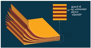
Over the past half-century, scientists have shaved silicon films down to just a wisp of atoms in pursuit of smaller, faster electronics. For the next set of breakthroughs, though, they’ll need novel ways to build even tinier and more powerful devices.
In a study published Sept. 20 in Nature, University of Chicago and Cornell University researchers describe an innovative method to make stacks of semiconductors just a few atoms thick. The technique offers scientists and engineers a simple, cost-effective method to make thin, uniform layers of these materials, which could expand capabilities for devices from solar cells to cell phones.
Stacking thin layers of materials offers a range of possibilities for making electronic devices with unique properties. But manufacturing such films is a delicate process, with little room for error.
“The scale of the problem we’re looking at is, imagine trying to lay down a flat sheet of plastic wrap the size of Chicago without getting any air bubbles in it,” said Jiwoong Park, a UChicago professor in the Department of Chemistry, the Institute for Molecular Engineering and the James Franck Institute, who led the study. “When the material itself is just atoms thick, every little stray atom is a problem.”
Today, these layers are “grown” instead of stacking them on top of one another. But that means the bottom layers have to be subjected to harsh growth conditions such as high temperatures while the new ones are added—a process that limits the materials with which to make them.
Park’s team instead made the films individually. Then they put them into a vacuum, peeled them off and stuck them to one another, like Post-It notes. This allowed the scientists to make films that were connected with weak bonds instead of stronger covalent bonds—interfering less with the perfect surfaces between the layers.
“The films, vertically controlled at the atomic-level, are exceptionally high-quality over entire wafers,” said Kibum Kang, a postdoctoral associate who was the first author of the study.
Kan-Heng Lee, a graduate student and co-first author of the study, then tested the films’ electrical properties by making them into devices and showed that their functions can be designed on the atomic scale, which could allow them to serve as the essential ingredient for future computer chips.
The method opens up a myriad of possibilities for such films. They can be made on top of water or plastics; they can be made to detach by dipping them into water; and they can be carved or patterned with an ion beam. Researchers are exploring the full range of what can be done with the method, which they said is simple and cost-effective.
“We expect this new method to accelerate the discovery of novel materials, as well as enabling large-scale manufacturing,” Park said.
Share on:


Testimonial
"The I-Connect007 team is outstanding—kind, responsive, and a true marketing partner. Their design team created fresh, eye-catching ads, and their editorial support polished our content to let our brand shine. Thank you all! "
Sweeney Ng - CEE PCBSuggested Items
September 2025 PCB007 Magazine: The Future of Advanced Materials
09/16/2025 | I-Connect007 Editorial TeamMoore’s Law is no more, and the advanced material solutions being developed to grapple with this reality are surprising, stunning, and perhaps a bit daunting. Buckle up for a dive into advanced materials and a glimpse into the next chapters of electronics manufacturing.
I-Connect007 Launches Advanced Electronics Packaging Digest
09/15/2025 | I-Connect007I-Connect007 is pleased to announce the launch of Advanced Electronics Packaging Digest (AEPD), a new monthly digital newsletter dedicated to one of the most critical and rapidly evolving areas of electronics manufacturing: advanced packaging at the interconnect level.
Panasonic Industry will Double the Production Capacity of MEGTRON Multi-layer Circuit Board Materials Over the Next Five Years
09/15/2025 | Panasonic Industry Co., Ltd.Panasonic Industry Co., Ltd., a Panasonic Group company, announced plans for a major expansion of its global production capacity for MEGTRON multi-layer circuit board materials today. The company plans to double its production over the next five years to meet growing demand in the AI server and ICT infrastructure markets.
Trouble in Your Tank: Implementing Direct Metallization in Advanced Substrate Packaging
09/15/2025 | Michael Carano -- Column: Trouble in Your TankDirect metallization systems based on conductive graphite are gaining popularity throughout the world. The environmental and productivity gains achievable with this process are outstanding. Direct metallization reduces the costs of compliance, waste treatment, and legal issues related to chemical exposure. A graphite-based direct plate system has been devised to address these needs.
Fresh PCB Concepts: Designing for Success at the Rigid-flex Transition Area
08/28/2025 | Team NCAB -- Column: Fresh PCB ConceptsRigid-flex PCBs come in all shapes and sizes. Manufacturers typically use fire-retardant, grade 4 (FR-4) materials in the rigid section and flexible polyimide materials in the flex region. Because of the small size, some rigid-flex PCBs, like those for hearing aid devices, are among the most challenging to manufacture. However, regardless of its size, we should not neglect the transition area between the rigid and flexible material.