


 Trouble in Your Tank: Implementing Direct Metallization in Advanced Substrate Packaging
 It’s Only Common Sense: Storytelling That Sells—Stop Pitching, Start Painting Pictures
 The Right Approach: Get Ready for ISO 9001 Version 6


A Little Tension Yields Enormous Solar Crystals
September 26, 2017 | KAUSTEstimated reading time: 2 minutes
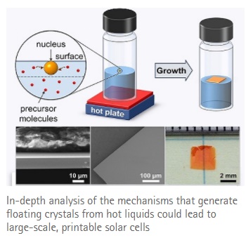
In the race to replace silicon in low-cost solar cells, semiconductors known as metal halide perovskites are favored because they can be solution-processed into thin films with excellent photovoltaic efficiency. A collaboration between KAUST and Oxford University researchers has now uncovered a strategy that grows perovskites into centimeter-scale, highly pure crystals thanks to the effect of surface tension.
In their natural state, perovskites have difficultly moving solar-generated electricity because they crystallize with randomly oriented grains. Osman Bakr from KAUST’s Solar Center and coworkers are working on ways to dramatically speed up the flow of these charge carriers using inverse temperature crystallization (ITC). This technique uses special organic liquids and thermal energy to force perovskites to solidify into structures resembling single crystals—the optimal arrangements for device purposes.
While ITC produces high-quality perovskites far faster than conventional chemical methods, the curious mechanisms that initiate crystallization in hot organic liquids are poorly understood. Ayan Zhumekenov, a PhD student in Bakr’s group, recalls spotting a key piece of evidence during efforts to adapt ITC toward large-scale manufacturing. “At some point, we realized that when crystals appeared, it was usually at the solution’s surface,” he says. “And this was particularly true when we used concentrated solutions.”
The KAUST team partnered with Oxford theoreticians to identify how interfaces influence perovskite growth in ITC. They propose that metal halides and solvent molecules initially cling together in tight complexes that begin to stretch and weaken at higher temperatures. With sufficient thermal energy, the complex breaks and perovskites begin to crystallize.
But interestingly, the researchers found that complexes located at the solution surface can experience additional forces due to surface tension—the strong cohesive forces that enable certain insects to stride over lakes and ponds. The extra pull provided by the surface makes it much easier to separate the solvent-perovskite complexes and nucleate crystals that float on top of the liquid.
Exploiting this knowledge helped the team produce centimeter-sized, ultrathin single crystals and prototype a photodetector with characteristics comparable to state-of-the-art devices. Although the single crystals are currently fragile and difficult to handle due to their microscale thicknesses, Zhumekenov explains that this method could help direct the perovskite growth onto specific substrates.
“Taking into account the roles of interfaces and surface tension could have a fundamental impact,” he says, “we can get large-area growth, and it’s not limited to specific metal cations—you could have a library of materials with perovskite structures.”
Share on:


Testimonial
"We’re proud to call I-Connect007 a trusted partner. Their innovative approach and industry insight made our podcast collaboration a success by connecting us with the right audience and delivering real results."
Julia McCaffrey - NCAB GroupSuggested Items
Driving Innovation: Depth Routing Processes—Achieving Unparalleled Precision in Complex PCBs
09/08/2025 | Kurt Palmer -- Column: Driving InnovationIn PCB manufacturing, the demand for increasingly complex and miniaturized designs continually pushes the boundaries of traditional fabrication methods, including depth routing. Success in these applications demands not only on robust machinery but also sophisticated control functions. PCB manufacturers rely on advanced machine features and process methodologies to meet their precise depth routing goals. Here, I’ll explore some crucial functions that empower manufacturers to master complex depth routing challenges.
Polar Instruments Announces Additive Transmission Line Support for Si9000e
08/20/2025 | Polar InstrumentsTransmission lines embedded into the PCB surface are a feature of UHDI constructions. The 2025 fall release of Polar's Si9000e PCB impedance & insertion loss transmission line field solver incorporates eight new single ended, differential and coplanar transmission line structures.
Henniker Plasma Launches Stratus Turnkey Plasma Manufacturing Cell
08/13/2025 | Henniker PlasmaHenniker Plasma, a leading manufacturer of plasma treatment systems, proudly announces the launch of its Stratus Plasma Manufacturing Cell range — a fully integrated, turnkey solution that combines advanced atmospheric plasma surface treatment with robotic automation.
Trouble in Your Tank: Metallizing Flexible Circuit Materials—Mitigating Deposit Stress
08/04/2025 | Michael Carano -- Column: Trouble in Your TankMetallizing materials, such as polyimide used for flexible circuitry and high-reliability multilayer printed wiring boards, provide a significant challenge for process engineers. Conventional electroless copper systems often require pre-treatments with hazardous chemicals or have a small process window to achieve uniform coverage without blistering. It all boils down to enhancing the adhesion of the thin film of electroless copper to these smooth surfaces.
Designers Notebook: Basic PCB Planning Criteria—Establishing Design Constraints
07/22/2025 | Vern Solberg -- Column: Designer's NotebookPrinted circuit board development flows more smoothly when all critical issues are predefined and understood from the start. As a basic planning strategy, the designer must first consider the product performance criteria, then determine the specific industry standards or specifications that the product must meet. Planning also includes a review of all significant issues that may affect the product’s manufacture, performance, reliability, overall quality, and safety.