


 Trouble in Your Tank: Implementing Direct Metallization in Advanced Substrate Packaging
 It’s Only Common Sense: Storytelling That Sells—Stop Pitching, Start Painting Pictures
 The Right Approach: Get Ready for ISO 9001 Version 6


Graphene Forged Into Three-Dimensional Shapes
September 28, 2017 | Academy of FinlandEstimated reading time: 2 minutes
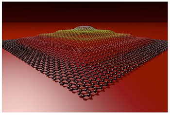
Researchers from Finland and Taiwan have discovered how graphene, a single-atom-thin layer of carbon, can be forged into three-dimensional objects by using laser light. A striking illustration was provided when the researchers fabricated a pyramid with a height of 60 nm, which is about 200 times larger than the thickness of a graphene sheet. The pyramid was so small that it would easily fit on a single strand of hair. The research was supported by the Academy of Finland and the Ministry of Science and Technology of the Republic of China.
Graphene is a close relative to graphite, which consists of millions of layers of graphene and can be found in common pencil tips. After graphene was first isolated in 2004, researchers have learned to routinely produce and handle it. Graphene can be used to make electronic and optoelectronic devices, such as transistors, photodetectors and sensors. In future, we will probably see an increasing number of products containing graphene.
“We call this technique optical forging, since the process resembles forging metals into 3D shapes with a hammer. In our case, a laser beam is the hammer that forges graphene into 3D shapes,” explains Professor Mika Pettersson, who led the experimental team at the Nanoscience Center of the University of Jyväskylä, Finland. “The beauty of the technique is that it’s fast and easy to use; it doesn’t require any additional chemicals or processing. Despite the simplicity of the technique, we were very surprised initially when we observed that the laser beam induced such substantial changes on graphene. It took a while to understand what was happening.”
“At first, we were flabbergasted. The experimental data simply made no sense,” says Dr Pekka Koskinen, who was responsible for the theory. “But gradually, by close interplay between experiments and computer simulations, the actuality of 3D shapes and their formation mechanism started to become clear.”
“When we first examined the irradiated graphene, we were expecting to find traces of chemical species incorporated into the graphene, but we couldn’t find any. After some more careful inspections, we concluded that it must be purely structural defects, rather than chemical doping, that are responsible for such dramatic changes on graphene,” explains Associate Professor Wei Yen Woon from Taiwan, who led the experimental group that carried out X-ray photoelectron spectroscopy at the synchrotron facility.
The novel 3D graphene is stable and it has electronic and optical properties that differ from normal 2D graphene. Optically forged graphene can help in fabricating 3D architectures for graphene-based devices.
The research was carried out at the Nanoscience Center (NSC) of the University of Jyväskylä, the National Central University of Taiwan and the National Synchrotron Radiation Research Center in Taiwan.
Share on:


Testimonial
"Advertising in PCB007 Magazine has been a great way to showcase our bare board testers to the right audience. The I-Connect007 team makes the process smooth and professional. We’re proud to be featured in such a trusted publication."
Klaus Koziol - atgSuggested Items
PC Graphics Add-in Board Shipments Up 27% QoQ in 2Q25
09/03/2025 | Jon Peddie ResearchAccording to a new research report from the analyst firm Jon Peddie Research, the growth of the global PC-based graphics add-in board market reached 11.6 million units in Q2'25 and desktop PC CPUs shipments increased to 21.7 million units.
PC GPU Shipments Up 8.4% in 2Q25 on Pre-Tariff Demand
09/02/2025 | Jon Peddie ResearchJon Peddie Research reports the growth of the global PC-based graphics processor unit (GPU) market reached 74.7 million units in Q2'25, and PC CPU shipments increased to 66.9 million units.
20 Years of Center Nanoelectronic Technologies (CNT) – Backbone of German Semiconductor Research Celebrates Anniversary
08/14/2025 | Fraunhofer IPMSThe Center Nanoelectronic Technologies (CNT) of the Fraunhofer Institute for Photonic Microsystems (IPMS) is celebrating its 20th anniversary this year. Since its founding in 2005, it has developed into a pillar of applied semiconductor research in Germany and Europe. With its unique research cleanroom and equipment adhering to the 300-mm wafer industry standard, CNT is unparalleled in Germany and serves as a central innovation driver for the microelectronics industry.
Q2 Client CPU Shipments Increased 8% from Last Quarter, Up 13% YoY
08/13/2025 | Jon Peddie ResearchJon Peddie Research reports that the global client CPU market expanded for two quarters in a row, and in Q2’25, it showed unseasonal growth of 7.9% from last quarter, while server CPU shipments increased 22% year over year.
FuriosaAI Closes $125M Investment Round to Scale Production of Next-Gen AI Inference Chip
07/31/2025 | BUSINESS WIREFuriosaAI, a semiconductor company building a new foundation for AI compute, today announced it has completed a $125 million Series C bridge funding round. The investment continues a period of significant momentum for Furiosa as global demand for high-performance, efficient AI infrastructure soars.