


 Trouble in Your Tank: Implementing Direct Metallization in Advanced Substrate Packaging
 It’s Only Common Sense: Storytelling That Sells—Stop Pitching, Start Painting Pictures
 The Right Approach: Get Ready for ISO 9001 Version 6


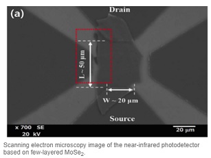
Advanced Molybdenum Selenide Near Infrared Phototransistors
September 29, 2017 | University of Electro-CommunicationsEstimated reading time: 1 minute
Optical sensors operating in the near infrared (NIR) are important for applications in imaging, photodetectors, and biological sensors. Notably, recent reports on the synthesis of high quality, large areas of graphene has motivated researchers to search for other 2D materials with properties suitable for NIR devices.
Now, Abdelkader Abderrahmane and colleagues at the University of Electro-Communications, Tokyo in collaboration with researchers at Chosun University, Korea, describe the optoelectronics characteristics of molybdenum selenide (MoSe2) phototransistors for applications to photodetectors. The application of gate voltages to the devices yielded a maximum photoresponsivity 238 A/W, an external quantum efficiency (EQE) of 37,745% under 785 nm light. The researchers state: "our device is one of the best high-performance nanoscale near-infrared photodetectors based on multilayered two-dimensional materials."
The devices were fabricated using few layered MoSe2 with a thickness of ~44 nm that was exfoliated from natural MoSe2 onto thermally oxidized silicon substrates with metallic strips acting as back gates. The transistor channel width and length were 50 and 20 μm, and the charge mobility was be 5.1 cm2 /V/s.
Electrical measurements indicated that the devices operated in the so-called accumulation mode and with a pinch off voltage of - 40V.
The combination of the 1.1 eV bandgap of MoSe2 and its high optical absorption compared to MoS2 is expected to offer wide ranging applications in optoelectronics.
Share on:


Testimonial
"Our marketing partnership with I-Connect007 is already delivering. Just a day after our press release went live, we received a direct inquiry about our updated products!"
Rachael Temple - AlltematedSuggested Items
MEMS & Imaging Sensors Summit to Spotlight Sensing Revolution for Europe’s Leadership
09/11/2025 | SEMIIndustry experts will gather November 19-20 at the SEMI MEMS & Imaging Sensors Summit 2025 to explore the latest breakthroughs in AI-driven MEMS and imaging optimization, AR/VR technologies, and advanced sensor solutions for critical defence applications.
Direct Imaging System Market Size to Hit $4.30B by 2032, Driven by Increasing Demand for High-Precision PCB Manufacturing
09/11/2025 | Globe NewswireAccording to the SNS Insider, “The Direct Imaging System Market size was valued at $2.21 Billion in 2024 and is projected to reach $4.30 Billion by 2032, growing at a CAGR of 8.68% during 2025-2032.”
I-Connect007’s Editor’s Choice: Five Must-Reads for the Week
07/04/2025 | Marcy LaRont, I-Connect007For our industry, we have seen several bullish market announcements over the past few weeks, including one this week by IDC on the massive growth in the global server market. We’re also closely watching global trade and nearshoring. One good example of successful nearshoring is Rehm Thermal Systems, which celebrates its 10th anniversary in Mexico and the official opening of its new building in Guadalajara.
Driving Innovation: Direct Imaging vs. Conventional Exposure
07/01/2025 | Simon Khesin -- Column: Driving InnovationMy first camera used Kodak film. I even experimented with developing photos in the bathroom, though I usually dropped the film off at a Kodak center and received the prints two weeks later, only to discover that some images were out of focus or poorly framed. Today, every smartphone contains a high-quality camera capable of producing stunning images instantly.
United Electronics Corporation Advances Manufacturing Capabilities with Schmoll MDI-ST Imaging Equipment
06/24/2025 | United Electronics CorporationUnited Electronics Corporation has successfully installed the advanced Schmoll MDI-ST (XL) imaging equipment at their advanced printed circuit board facility. This significant technology investment represents a continued commitment to delivering superior products and maintaining their position as an industry leader in precision PCB manufacturing.