


 Trouble in Your Tank: Implementing Direct Metallization in Advanced Substrate Packaging
 It’s Only Common Sense: Storytelling That Sells—Stop Pitching, Start Painting Pictures
 The Right Approach: Get Ready for ISO 9001 Version 6


Scientists Reveal Potential of Energy-Efficient Next-Gen Electronic Memory
October 13, 2017 | Berkeley LabEstimated reading time: 3 minutes
The same electrostatic charge that can make hair stand on end and attach balloons to clothing could be an efficient way to drive atomically thin electronic memory devices of the future, according to a new study led by researchers at the Department of Energy’s Lawrence Berkeley National Laboratory (Berkeley Lab).
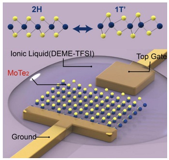
Schematic shows the configuration for structural phase transition on a molybdenum ditelluride monolayer (MoTe2, shown as yellow and blue spheres), which is anchored by a metal electrodes (top gate and ground). The ionic liquid covering the monolayer and electrodes enables a high density of electrons to populate the monolayer, leading to changes in the structural lattice from a hexagonal (2H) to monoclinic (1T’) pattern. (Credit: Ying Wang/Berkeley Lab)
In a study published today in the journal Nature, scientists have found a way to reversibly change the atomic structure of a 2-D material by injecting, or “doping,” it with electrons. The process uses far less energy than current methods for changing the configuration of a material’s structure.
“We show, for the first time, that it is possible to inject electrons to drive structural phase changes in materials,” said study principal investigator Xiang Zhang, senior faculty scientist at Berkeley Lab’s Materials Sciences Division and a professor at UC Berkeley. “By adding electrons into a material, the overall energy goes up and will tip off the balance, resulting in the atomic structure rearranging to a new pattern that is more stable. Such electron doping-driven structural phase transitions at the 2-D limit is not only important in fundamental physics; it also opens the door for new electronic memory and low-power switching in the next generation of ultra-thin devices.”
Switching a material’s structural configuration from one phase to another is the fundamental, binary characteristic that underlies today’s digital circuitry. Electronic components capable of this phase transition have shrunk down to paper-thin sizes, but they are still considered to be bulk, 3-D layers by scientists. By comparison, 2-D monolayer materials are composed of a single layer of atoms or molecules whose thickness is 100,000 times as small as a human hair.
“The idea of electron doping to alter a material’s atomic structure is unique to 2-D materials, which are much more electrically tunable compared with 3-D bulk materials,” said study co-lead author Jun Xiao, a graduate student in Zhang’s lab.
The classic approach to driving the structural transition of materials involves heating to above 500 degrees Celsius. Such methods are energy-intensive and not feasible for practical applications. In addition, the excess heat can significantly reduce the life span of components in integrated circuits.
A number of research groups have also investigated the use of chemicals to alter the configuration of atoms in semiconductor materials, but that process is still difficult to control and has not been widely adopted by industry.
“Here we use electrostatic doping to control the atomic configuration of a two-dimensional material,” said study co-lead author Ying Wang, another graduate student in Zhang’s lab. “Compared to the use of chemicals, our method is reversible and free of impurities. It has greater potential for integration into the manufacturing of cell phones, computers, and other electronic devices.”
The researchers used molybdenum ditelluride (MoTe2), a typical 2-D semiconductor, and coated it with an ionic liquid (DEME-TFSI), which has an ultra-high capacitance, or ability to store electric charges. The layer of ionic liquid allowed the researchers to inject the semiconductor with electrons at a density of a hundred trillion to a quadrillion per square centimeter. It is an electron density that is one to two orders higher in magnitude than what could be achieved in 3-D bulk materials, the researchers said.
Through spectroscopic analysis, the researchers determined that the injection of electrons changed the atoms’ arrangement of the molybdenum ditelluride from a hexagonal shape to one that is monoclinic, which has more of a slanted cuboid shape. Once the electrons were retracted, the crystal structure returned to its original hexagonal pattern, showing that the phase transition is reversible. Moreover, these two types of atom arrangements have very different symmetries, providing a large contrast for applications in optical components.
“Such an atomically thin device could have dual functions, serving simultaneously as optical or electrical transistors, and hence broaden the functionalities of the electronics used in our daily lives,” said Wang.
About Lawrence Berkeley National Laboratory
Lawrence Berkeley National Laboratory addresses the world’s most urgent scientific challenges by advancing sustainable energy, protecting human health, creating new materials, and revealing the origin and fate of the universe. Founded in 1931, Berkeley Lab’s scientific expertise has been recognized with 13 Nobel Prizes. The University of California manages Berkeley Lab for the U.S. Department of Energy’s Office of Science.
Share on:


Testimonial
"In a year when every marketing dollar mattered, I chose to keep I-Connect007 in our 2025 plan. Their commitment to high-quality, insightful content aligns with Koh Young’s values and helps readers navigate a changing industry. "
Brent Fischthal - Koh YoungSuggested Items
September 2025 PCB007 Magazine: The Future of Advanced Materials
09/16/2025 | I-Connect007 Editorial TeamMoore’s Law is no more, and the advanced material solutions being developed to grapple with this reality are surprising, stunning, and perhaps a bit daunting. Buckle up for a dive into advanced materials and a glimpse into the next chapters of electronics manufacturing.
I-Connect007 Launches Advanced Electronics Packaging Digest
09/15/2025 | I-Connect007I-Connect007 is pleased to announce the launch of Advanced Electronics Packaging Digest (AEPD), a new monthly digital newsletter dedicated to one of the most critical and rapidly evolving areas of electronics manufacturing: advanced packaging at the interconnect level.
Panasonic Industry will Double the Production Capacity of MEGTRON Multi-layer Circuit Board Materials Over the Next Five Years
09/15/2025 | Panasonic Industry Co., Ltd.Panasonic Industry Co., Ltd., a Panasonic Group company, announced plans for a major expansion of its global production capacity for MEGTRON multi-layer circuit board materials today. The company plans to double its production over the next five years to meet growing demand in the AI server and ICT infrastructure markets.
Trouble in Your Tank: Implementing Direct Metallization in Advanced Substrate Packaging
09/15/2025 | Michael Carano -- Column: Trouble in Your TankDirect metallization systems based on conductive graphite are gaining popularity throughout the world. The environmental and productivity gains achievable with this process are outstanding. Direct metallization reduces the costs of compliance, waste treatment, and legal issues related to chemical exposure. A graphite-based direct plate system has been devised to address these needs.
Fresh PCB Concepts: Designing for Success at the Rigid-flex Transition Area
08/28/2025 | Team NCAB -- Column: Fresh PCB ConceptsRigid-flex PCBs come in all shapes and sizes. Manufacturers typically use fire-retardant, grade 4 (FR-4) materials in the rigid section and flexible polyimide materials in the flex region. Because of the small size, some rigid-flex PCBs, like those for hearing aid devices, are among the most challenging to manufacture. However, regardless of its size, we should not neglect the transition area between the rigid and flexible material.