


 Trouble in Your Tank: Implementing Direct Metallization in Advanced Substrate Packaging
 It’s Only Common Sense: Storytelling That Sells—Stop Pitching, Start Painting Pictures
 The Right Approach: Get Ready for ISO 9001 Version 6


IC Makers Maximize 300mm, 200mm Wafer Capacity
October 13, 2017 | IC InsightsEstimated reading time: 1 minute
With the prospects of large 450mm wafers going nowhere, IC manufacturers are increasing efforts to maximize fabrication plants using 300mm and 200mm diameter silicon substrates. The number of 300mm wafer production-class fabs in operation worldwide is expected to increase each year between now and 2021 to reach 123 compared to 98 in 2016, according to the forecast in IC Insights’ Global Wafer Capacity 2017-2021 report.
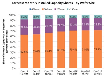
As shown in the figure, 300mm wafers represented 63.6% of worldwide IC fab capacity at the end of 2016 and are projected to reach 71.2% by the end of 2021, which translates into a compound annual growth rate (CAGR) of 8.1% in terms of silicon area for processing by plant equipment in the five-year period.
The report’s count of 98 production-class 300mm fabs in use worldwide at the end of 2016 excludes numerous R&D front-end lines and a few high-volume 300mm plants that make non-IC semiconductors (such as power transistors). Currently, there are eight 300mm wafer fabs that have opened or are scheduled to open in 2017, which is the highest number in one year since 2014 when seven were added, says the Global Wafer Capacity report. Another nine are scheduled to open in 2018. Virtually all these new fabs will be for DRAM, flash memory, or foundry capacity, according to the report.
Even though 300mm wafers are now the majority wafer size in use, both in terms of total surface area and in actual quantity of wafers, there is still much life remaining in 200mm fabs, the capacity report concludes. IC production capacity on 200mm wafers is expected to increase every year through 2021, growing at a CAGR of 1.1% in terms of total available silicon area. However, the share of the IC industry’s monthly wafer capacity represented by 200mm wafers is forecast to drop from 28.4% in 2016 to 22.8% in 2021.
IC Insights believes there is still much life left in 200mm fabs because not all semiconductor devices are able to take advantage of the cost savings 300mm wafers can provide. Fabs running 200mm wafers will continue to be profitable for many more years for the fabrication of numerous types of ICs, such as specialty memories, display drivers, microcontrollers, and RF and analog products. In addition, 200mm fabs are also used for manufacturing MEMS-based “non-IC” products such as accelerometers, pressure sensors, and actuators, including acoustic-wave RF filtering devices and micro-mirror chips for digital projectors and displays, as well as power discrete semiconductors and some high-brightness LEDs.
Share on:


Testimonial
"The I-Connect007 team is outstanding—kind, responsive, and a true marketing partner. Their design team created fresh, eye-catching ads, and their editorial support polished our content to let our brand shine. Thank you all! "
Sweeney Ng - CEE PCBSuggested Items
Panasonic Industry will Double the Production Capacity of MEGTRON Multi-layer Circuit Board Materials Over the Next Five Years
09/15/2025 | Panasonic Industry Co., Ltd.Panasonic Industry Co., Ltd., a Panasonic Group company, announced plans for a major expansion of its global production capacity for MEGTRON multi-layer circuit board materials today. The company plans to double its production over the next five years to meet growing demand in the AI server and ICT infrastructure markets.
VIDEOTON EAS's Bulgarian Subsidiary Expands Into Automotive Products
09/15/2025 | VideotonVEAS Bulgaria, engaged in electronics manufacturing, has joined the ranks of VIDEOTON companies authorized to produce automotive products.
Variosystems Strengthens North American Presence with Southlake Relaunch 2025
09/15/2025 | VariosystemsVariosystems celebrated the relaunch of its U.S. facility in Southlake, Texas. After months of redesign and reorganization, the opening marked more than just the return to a modernized production site—it was a moment to reconnect with our teams, partners, and the local community.
Integrating Uniplate PLBCu6 With the Digital Factory Suite
09/12/2025 | Giovanni Obino and Andreas Schatz, MKS' AtotechPrinted circuit board manufacturing is rapidly changing, driven by miniaturization, stringent reliability requirements, and growing pressure for sustainable production. Meeting these challenges requires more than incremental improvements; it demands a combination of precise equipment and real-time process intelligence. The pairing of Uniplate® PLBCu6 with the Digital Factory Suite (DFS) demonstrates how hardware and software can work together to create more responsive, resource-efficient manufacturing.
United Electronics Corporation Unveils Revolutionary CIMS Galaxy 30 Automated Optical Inspection System
09/11/2025 | United Electronics CorporationUnited Electronics Corporation (UEC) today announced the launch of its new groundbreaking CIMS Galaxy 30 Automated Optical Inspection (AOI) machine, setting a new industry standard for precision electronics manufacturing quality control. The Galaxy 30, developed and manufactured by CIMS, represents a significant leap forward in inspection technology, delivering exceptional speed improvements and introducing cutting-edge artificial intelligence capabilities.