


 Trouble in Your Tank: Implementing Direct Metallization in Advanced Substrate Packaging
 It’s Only Common Sense: Storytelling That Sells—Stop Pitching, Start Painting Pictures
 The Right Approach: Get Ready for ISO 9001 Version 6


New Method to Detect Spin Current in Quantum Materials Unlocks Potential for Alternative Electronics
October 16, 2017 | ORNLEstimated reading time: 3 minutes
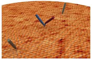
A new method that precisely measures the mysterious behavior and magnetic properties of electrons flowing across the surface of quantum materials could open a path to next-generation electronics.
Found at the heart of electronic devices, silicon-based semiconductors rely on the controlled electrical current responsible for powering electronics. These semiconductors can only access the electrons’ charge for energy, but electrons do more than carry a charge. They also have intrinsic angular momentum known as spin, which is a feature of quantum materials that, while elusive, can be manipulated to enhance electronic devices.
A team of scientists, led by An-Ping Li at the Department of Energy’s Oak Ridge National Laboratory, has developed an innovative microscopy technique to detect the spin of electrons in topological insulators, a new kind of quantum material that could be used in applications such as spintronics and quantum computing.
“The spin current, namely the total angular momentum of moving electrons, is a behavior in topological insulators that could not be accounted for until a spin-sensitive method was developed,” Li said.
Electronic devices continue to evolve rapidly and require more power packed into smaller components. This prompts the need for less costly, energy-efficient alternatives to charge-based electronics. A topological insulator carries electrical current along its surface, while deeper within the bulk material, it acts as an insulator. Electrons flowing across the material’s surface exhibit uniform spin directions, unlike in a semiconductor where electrons spin in varying directions.
“Charge-based devices are less energy efficient than spin-based ones,” said Li. “For spins to be useful, we need to control both their flow and orientation.”
To detect and better understand this quirky particle behavior, the team needed a method sensitive to the spin of moving electrons. Their new microscopy approach was tested on a single crystal of Bi2Te2Se, a material containing bismuth, tellurium and selenium. It measured how much voltage was produced along the material’s surface as the flow of electrons moved between specific points while sensing the voltage for each electron’s spin.
The new method builds on a four-probe scanning tunneling microscope—an instrument that can pinpoint a material’s atomic activity with four movable probing tips—by adding a component to observe the spin behavior of electrons on the material’s surface. This approach not only includes spin sensitivity measurements. It also confines the current to a small area on the surface, which helps to keep electrons from escaping beneath the surface, providing high-resolution results.
“We successfully detected a voltage generated by the electron’s spin current,” said Li, who coauthored a paper published by Physical Review Letters that explains the method. “This work provides clear evidence of the spin current in topological insulators and opens a new avenue to study other quantum materials that could ultimately be applied in next-generation electronic devices.”
Additional coauthors of the study titled, “Detection of the Spin-Chemical Potential in Topological Insulators Using Spin-Polarized Four-Probe STM,” include ORNL’s Saban Hus, Giang Nguyen, Wonhee Ko and Arthur Baddorf; X.-G. Zhang of the University of Florida; and Yong Chen of Purdue University.
This research was conducted at the Center for Nanophase Materials Sciences, a DOE Office of Science User Facility. The development of the novel microscopy method was funded by ORNL’s Laboratory Directed Research and Development program.
ORNL is managed by UT-Battelle for DOE’s Office of Science. The Office of Science is the single largest supporter of basic research in the physical sciences in the United States, and is working to address some of the most pressing challenges of our time. For more information, please click here.
Share on:


Testimonial
"Advertising in PCB007 Magazine has been a great way to showcase our bare board testers to the right audience. The I-Connect007 team makes the process smooth and professional. We’re proud to be featured in such a trusted publication."
Klaus Koziol - atgSuggested Items
September 2025 PCB007 Magazine: The Future of Advanced Materials
09/16/2025 | I-Connect007 Editorial TeamMoore’s Law is no more, and the advanced material solutions being developed to grapple with this reality are surprising, stunning, and perhaps a bit daunting. Buckle up for a dive into advanced materials and a glimpse into the next chapters of electronics manufacturing.
I-Connect007 Launches Advanced Electronics Packaging Digest
09/15/2025 | I-Connect007I-Connect007 is pleased to announce the launch of Advanced Electronics Packaging Digest (AEPD), a new monthly digital newsletter dedicated to one of the most critical and rapidly evolving areas of electronics manufacturing: advanced packaging at the interconnect level.
Panasonic Industry will Double the Production Capacity of MEGTRON Multi-layer Circuit Board Materials Over the Next Five Years
09/15/2025 | Panasonic Industry Co., Ltd.Panasonic Industry Co., Ltd., a Panasonic Group company, announced plans for a major expansion of its global production capacity for MEGTRON multi-layer circuit board materials today. The company plans to double its production over the next five years to meet growing demand in the AI server and ICT infrastructure markets.
Trouble in Your Tank: Implementing Direct Metallization in Advanced Substrate Packaging
09/15/2025 | Michael Carano -- Column: Trouble in Your TankDirect metallization systems based on conductive graphite are gaining popularity throughout the world. The environmental and productivity gains achievable with this process are outstanding. Direct metallization reduces the costs of compliance, waste treatment, and legal issues related to chemical exposure. A graphite-based direct plate system has been devised to address these needs.
Fresh PCB Concepts: Designing for Success at the Rigid-flex Transition Area
08/28/2025 | Team NCAB -- Column: Fresh PCB ConceptsRigid-flex PCBs come in all shapes and sizes. Manufacturers typically use fire-retardant, grade 4 (FR-4) materials in the rigid section and flexible polyimide materials in the flex region. Because of the small size, some rigid-flex PCBs, like those for hearing aid devices, are among the most challenging to manufacture. However, regardless of its size, we should not neglect the transition area between the rigid and flexible material.