


 Trouble in Your Tank: Implementing Direct Metallization in Advanced Substrate Packaging
 It’s Only Common Sense: Storytelling That Sells—Stop Pitching, Start Painting Pictures
 The Right Approach: Get Ready for ISO 9001 Version 6


Invention Could Potentially Make Microprocessor Chips Work 1,000 Times Faster
October 20, 2017 | NUSEstimated reading time: 2 minutes
Advancement in nanoelectronics, which is the use of nanotechnology in electronic components, has been fueled by the ever-increasing need to shrink the size of electronic devices in a bid to produce smaller, faster and smarter gadgets such as computers, memory storage devices, displays and medical diagnostic tools.
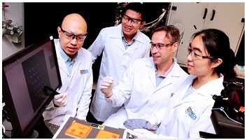
A research team led by Associate Professor Christian Nijhuis from the Department of Chemistry at the NUS Faculty of Science (second from right) has recently invented a novel “converter” that can harness the speed and small size of plasmons for high frequency data processing and transmission in nanoelectronics.
While most advanced electronic devices are powered by photonics – which involves the use of photons to transmit information – photonic elements are usually large in size and this greatly limits their use in many advanced nanoelectronics systems.
Plasmons, which are waves of electrons that move along the surface of a metal after it is struck by photons, holds great promise for disruptive technologies in nanoelectronics. They are comparable to photons in terms of speed (they also travel with the speed of light), and they are much smaller. This unique property of plasmons makes them ideal for integration with nanoelectronics. However, earlier attempts to harness plasmons as information carriers had little success.
Addressing this technological gap, a research team from the National University of Singapore (NUS) has recently invented a novel “converter” that can harness the speed and small size of plasmons for high frequency data processing and transmission in nanoelectronics.
“This innovative transducer can directly convert electrical signals into plasmonic signals, and vice versa, in a single step. By bridging plasmonics and nanoscale electronics, we can potentially make chips run faster and reduce power losses. Our plasmonic-electronic transducer is about 10,000 times smaller than optical elements. We believe it can be readily integrated into existing technologies and can potentially be used in a wide range of applications in the future,” explained Associate Professor Christian Nijhuis from the Department of Chemistry at the NUS Faculty of Science, who is the leader of the research team behind this breakthrough.
From electricity to plasmons in one single step
In most techniques in plasmonics, plasmons are excited in two steps – electrons are used to generate light, which in turn is used to excite plasmons. To convert electrical signals into plasmonic signals, and vice versa, in one single step, the NUS team employed a process called tunnelling, in which electrons travel from one electrode to another electrode, and by doing so, excite plasmons.
“The two-step process is time-consuming and inefficient. Our technology stands out as we provide a one-stop solution for the conversion electrical signals to plasmonic signals. This can be achieved without a light source, which requires multiple-steps and large optical elements, complicating integration with nanoelectronics. Based on our lab experiments, the electron-to-plasmon conversion has an efficiency of more than 10%, more than 1,000 times higher than previously reported,” added Assoc Prof Nijhuis, who is also from the NUS Centre for Advanced 2D Materials and NUS Nanoscience and Nanotechnology Institute.
This groundbreaking work was conducted in collaboration with Dr Chu Hong Son from the Institute of High Performance Computing under the Agency for Science, Technology and Research.
Industry partnership and further studies
The research team has filed four patents for their invention, and is collaborating with industry partners to integrate the plasmonic-electronic “converters” with existing technologies.
The researchers plan to conduct further studies to reduce the size of the device so that it can operate at much higher frequencies. The team is also working on integrating the transducers with more efficient plasmonic waveguides for better performance.
Share on:


Testimonial
"In a year when every marketing dollar mattered, I chose to keep I-Connect007 in our 2025 plan. Their commitment to high-quality, insightful content aligns with Koh Young’s values and helps readers navigate a changing industry. "
Brent Fischthal - Koh YoungSuggested Items
Advint Incorporated Brings Artificial Intelligence to Electroplating Training
09/11/2025 | Advint IncorporatedAdvint Incorporated is introducing a new dimension to its electroplating training programs: the integration of Artificial Intelligence (AI). This initiative reflects the company’s commitment to providing PCB fabricators and manufacturers in the USA and Canada with training that is practical, forward-looking, and directly relevant to today’s production challenges.
The Signal Integrity Issue: Design007 Magazine September 2025
09/09/2025 | I-Connect007 Editorial TeamAs the saying goes, “If you don’t have signal integrity problems now, you will eventually.” This month, our experts share a variety of design techniques that can help PCB designers and design engineers achieve signal integrity.
Semiconductors Get Magnetic Boost with New Method from UCLA Researchers
07/31/2025 | UCLA NewsroomA new method for combining magnetic elements with semiconductors — which are vital materials for computers and other electronic devices — was unveiled by a research team led by the California NanoSystems Institute at UCLA.
SMT Perspectives and Prospects: Warren Buffett’s Perpetual Wisdom, Part 1
07/29/2025 | Dr. Jennie Hwang -- Column: SMT Perspectives and ProspectsOver the years, I have cherished the lessons by Warren Buffett and Charlie Munger at the Berkshire Hathaway annual shareholders meeting in Omaha, Nebraska. This year, I was among the more than 40,000 who attended the May 3 meeting. Millions more from around the world, including from the UK, Germany, Japan, China, Panama, and Guatemala, tuned in remotely and via CNBC’s livestream.
Mesa West, Advanced West Announce Strategic Partnership
06/15/2025 | I-Connect007Mesa West is proud to announce that they have officially joined forces with Advanced West. This strategic partnership brings together two industry leaders, uniting strengths to better serve customers through enhanced capabilities, expanded offerings, and continued commitment to quality.