


 Trouble in Your Tank: Implementing Direct Metallization in Advanced Substrate Packaging
 It’s Only Common Sense: Storytelling That Sells—Stop Pitching, Start Painting Pictures
 The Right Approach: Get Ready for ISO 9001 Version 6


Turning a Pinch of Salt Into an Electrical Switch
October 24, 2017 | University of LiverpoolEstimated reading time: 2 minutes
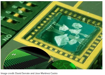
A team of scientists from the University of Liverpool, University College London and the University of Zaragoza in Spain has discovered a way to induce and control a fundamental electrical switching behaviour on the nano-scale.
Their results are reported in the journal Nature Nanotechnology, where the team describe how separating an atomically thin layer of rock salt material – including ordinary table salt – from the surface of metallic copper by including an atomically thin layer of copper nitride in between creates a layer of so-called “electric dipoles”, whose orientation can be switched by applying a large electric field.
When most materials are turned upside-down, they look the same at the atomic level and the electrical charges in the atoms cannot have a preference for orienting along a particular direction. In some materials, however, this symmetry is broken, and these charges can line up to form electric dipoles, which can be switched between multiple orientations with an electric field. If they remain in the same orientation after the electric field is removed, the material is commonly referred to as a ferroelectric which is the electrical analogue of a ferromagnet.
Because of the intrinsic switching behaviour of ferroelectrics there is a great interest in using nanoscale ferroelectrics for a new form of high density data storage. However, the outermost layers of a ferroelectric material often lose their ability to switch when they are incorporated into an electrical circuit. This makes it difficult to scale ferroelectric materials down to the atomic scale.
To overcome these difficulties, the scientists explored whether the new emergent properties of two-dimensional (2D) materials which are only a few atomic layers thick could be exploited to create a different kind of dipolar switching material. These materials, can have properties that are dramatically different from those of their thicker counterparts.
The team started by forming an atomically thin layer of nitrogen and copper (copper nitride) on the surface of a copper crystal. On top of this, they deposited an atomically thin layer of rock salt material, specifically sodium chloride (ordinary table salt) and potassium bromide, which do not have net dipoles.
Professor Mats Persson, from the University’s Department of Chemistry and the theorist of the paper, said: “This is a very exciting development and contrary to traditional wisdom that it is possible to have ferroelectric-like behaviour in atomically, thin layers in a metal-insulator junction”.
Many of the most promising proposed applications for 2D materials involve incorporating them into electrical circuits, so much attention has been focused on conducting 2D materials. However, 2D insulators are beginning to play an increasingly important role.
“By stacking two 2D materials, even those that are insulators, we can create new behaviour that neither material would be able to exhibit individually. This opens a wealth of new possibilities for developing a new generation of 2D material structures.” remarked Cyrus Hirjibehedin, the project’s lead scientist.
Share on:


Testimonial
"Our marketing partnership with I-Connect007 is already delivering. Just a day after our press release went live, we received a direct inquiry about our updated products!"
Rachael Temple - AlltematedSuggested Items
Trouble in Your Tank: Implementing Direct Metallization in Advanced Substrate Packaging
09/15/2025 | Michael Carano -- Column: Trouble in Your TankDirect metallization systems based on conductive graphite are gaining popularity throughout the world. The environmental and productivity gains achievable with this process are outstanding. Direct metallization reduces the costs of compliance, waste treatment, and legal issues related to chemical exposure. A graphite-based direct plate system has been devised to address these needs.
Closing the Loop on PCB Etching Waste
09/09/2025 | Shawn Stone, IECAs the PCB industry continues its push toward greener, more cost-efficient operations, Sigma Engineering’s Mecer System offers a comprehensive solution to two of the industry’s most persistent pain points: etchant consumption and rinse water waste. Designed as a modular, fully automated platform, the Mecer System regenerates spent copper etchants—both alkaline and acidic—and simultaneously recycles rinse water, transforming a traditionally linear chemical process into a closed-loop system.
Driving Innovation: Depth Routing Processes—Achieving Unparalleled Precision in Complex PCBs
09/08/2025 | Kurt Palmer -- Column: Driving InnovationIn PCB manufacturing, the demand for increasingly complex and miniaturized designs continually pushes the boundaries of traditional fabrication methods, including depth routing. Success in these applications demands not only on robust machinery but also sophisticated control functions. PCB manufacturers rely on advanced machine features and process methodologies to meet their precise depth routing goals. Here, I’ll explore some crucial functions that empower manufacturers to master complex depth routing challenges.
Trouble in Your Tank: Minimizing Small-via Defects for High-reliability PCBs
08/27/2025 | Michael Carano -- Column: Trouble in Your TankTo quote the comedian Stephen Wright, “If at first you don’t succeed, then skydiving is not for you.” That can be the battle cry when you find that only small-diameter vias are exhibiting voids. Why are small holes more prone to voids than larger vias when processed through electroless copper? There are several reasons.
The Government Circuit: Navigating New Trade Headwinds and New Partnerships
08/25/2025 | Chris Mitchell -- Column: The Government CircuitAs global trade winds continue to howl, the electronics manufacturing industry finds itself at a critical juncture. After months of warnings, the U.S. Government has implemented a broad array of tariff increases, with fresh duties hitting copper-based products, semiconductors, and imports from many nations. On the positive side, tentative trade agreements with Europe, China, Japan, and other nations are providing at least some clarity and counterbalance.