


 Trouble in Your Tank: Implementing Direct Metallization in Advanced Substrate Packaging
 It’s Only Common Sense: Storytelling That Sells—Stop Pitching, Start Painting Pictures
 The Right Approach: Get Ready for ISO 9001 Version 6


Taming 'Wild' Electrons in Graphene
October 25, 2017 | Rutgers UniversityEstimated reading time: 2 minutes
Graphene – a one-atom-thick layer of the stuff in pencils – is a better conductor than copper and is very promising for electronic devices, but with one catch: Electrons that move through it can’t be stopped.
Until now, that is. Scientists at Rutgers University-New Brunswick have learned how to tame the unruly electrons in graphene, paving the way for the ultra-fast transport of electrons with low loss of energy in novel systems. Their study was published online in Nature Nanotechnology.
“This shows we can electrically control the electrons in graphene,” said Eva Y. Andrei, Board of Governors professor in Rutgers’ Department of Physics and Astronomy in the School of Arts and Sciences and the study’s senior author. “In the past, we couldn’t do it. This is the reason people thought that one could not make devices like transistors that require switching with graphene, because their electrons run wild.”
Now it may become possible to realize a graphene nano-scale transistor, Andrei said. Thus far, graphene electronics components include ultrafast amplifiers, supercapacitors and ultralow resistivity wires. The addition of a graphene transistor would be an important step towards an all-graphene electronics platform. Other graphene-based applications include ultrasensitive chemical and biological sensors, filters for desalination and water purification. Graphene is also being developed in flat flexible screens, and paintable and printable electronic circuits.
Graphene is a nano-thin layer of the carbon-based graphite that pencils write with. It is far stronger than steel and a great conductor. But when electrons move through it, they do so in straight lines and their high velocity does not change. “If they hit a barrier, they can’t turn back, so they have to go through it,” Andrei said. “People have been looking at how to control or tame these electrons.”
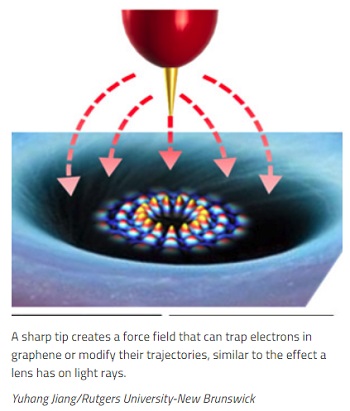
Her team managed to tame these wild electrons by sending voltage through a high-tech microscope with an extremely sharp tip, also the size of one atom. They created what resembles an optical system by sending voltage through a scanning tunneling microscope, which offers 3-D views of surfaces at the atomic scale. The microscope’s sharp tip creates a force field that traps electrons in graphene or modifies their trajectories, similar to the effect a lens has on light rays. Electrons can easily be trapped and released, providing an efficient on-off switching mechanism, according to Andrei.
“You can trap electrons without making holes in the graphene,” she said. “If you change the voltage, you can release the electrons. So you can catch them and let them go at will.”
The next step would be to scale up by putting extremely thin wires, called nanowires, on top of graphene and controlling the electrons with voltages, she said.
The study’s co-lead authors are Yuhang Jiang and Jinhai Mao, Rutgers postdoctoral fellows, and a graduate student at Universiteit Antwerpen in Belgium. The other Rutgers co-author is Guohong Li, a research associate.
Share on:


Testimonial
"Advertising in PCB007 Magazine has been a great way to showcase our bare board testers to the right audience. The I-Connect007 team makes the process smooth and professional. We’re proud to be featured in such a trusted publication."
Klaus Koziol - atgSuggested Items
Trouble in Your Tank: Implementing Direct Metallization in Advanced Substrate Packaging
09/15/2025 | Michael Carano -- Column: Trouble in Your TankDirect metallization systems based on conductive graphite are gaining popularity throughout the world. The environmental and productivity gains achievable with this process are outstanding. Direct metallization reduces the costs of compliance, waste treatment, and legal issues related to chemical exposure. A graphite-based direct plate system has been devised to address these needs.
Closing the Loop on PCB Etching Waste
09/09/2025 | Shawn Stone, IECAs the PCB industry continues its push toward greener, more cost-efficient operations, Sigma Engineering’s Mecer System offers a comprehensive solution to two of the industry’s most persistent pain points: etchant consumption and rinse water waste. Designed as a modular, fully automated platform, the Mecer System regenerates spent copper etchants—both alkaline and acidic—and simultaneously recycles rinse water, transforming a traditionally linear chemical process into a closed-loop system.
Driving Innovation: Depth Routing Processes—Achieving Unparalleled Precision in Complex PCBs
09/08/2025 | Kurt Palmer -- Column: Driving InnovationIn PCB manufacturing, the demand for increasingly complex and miniaturized designs continually pushes the boundaries of traditional fabrication methods, including depth routing. Success in these applications demands not only on robust machinery but also sophisticated control functions. PCB manufacturers rely on advanced machine features and process methodologies to meet their precise depth routing goals. Here, I’ll explore some crucial functions that empower manufacturers to master complex depth routing challenges.
Trouble in Your Tank: Minimizing Small-via Defects for High-reliability PCBs
08/27/2025 | Michael Carano -- Column: Trouble in Your TankTo quote the comedian Stephen Wright, “If at first you don’t succeed, then skydiving is not for you.” That can be the battle cry when you find that only small-diameter vias are exhibiting voids. Why are small holes more prone to voids than larger vias when processed through electroless copper? There are several reasons.
The Government Circuit: Navigating New Trade Headwinds and New Partnerships
08/25/2025 | Chris Mitchell -- Column: The Government CircuitAs global trade winds continue to howl, the electronics manufacturing industry finds itself at a critical juncture. After months of warnings, the U.S. Government has implemented a broad array of tariff increases, with fresh duties hitting copper-based products, semiconductors, and imports from many nations. On the positive side, tentative trade agreements with Europe, China, Japan, and other nations are providing at least some clarity and counterbalance.