


 Trouble in Your Tank: Implementing Direct Metallization in Advanced Substrate Packaging
 It’s Only Common Sense: Storytelling That Sells—Stop Pitching, Start Painting Pictures
 The Right Approach: Get Ready for ISO 9001 Version 6


New Property Found in Unusual Crystalline Materials
October 26, 2017 | MITEstimated reading time: 4 minutes
Most metals and semiconductors, from the steel in a knife blade to the silicon in a solar panel, are made up of many tiny crystalline grains. The way these grains meet at their edges can have a major impact on the solid’s properties, including mechanical strength, electrical conductivity, thermal properties, flexibility, and so on.
When the boundaries between the grains are of a particular type, called a coherent twin boundary (CTB), this adds useful properties to certain materials, especially at the nanoscale. It increases their strength, making the material much stronger while preserving its ability to be deformed, unlike most other processes that add strength. Now, researchers have discovered a new deformation mechanism of these twin crystal boundaries, which could help engineers figure out how to more precisely use CTBs to tune the properties of some materials.
Contrary to expectations, it turns out that a material’s crystal grains can sometimes slide along these CTBs. The new finding is described in a paper published this week in the journal Nature Communications by Ming Dao, a principal research scientist in MIT’s Department of Materials Science and Engineering; Subra Suresh, the Vannevar Bush Professor Emeritus of Engineering and president-designate of Nanyang Technological University in Singapore; Ju Li, the Battelle Energy Alliance Professor in MIT’s Department of Nuclear Science and Engineering; and seven others at MIT and elsewhere.
While each crystal grain is made up of an orderly three-dimensional array of atoms in a lattice structure, CTBs are places where, on the two sides of a boundary, the lattice forms a mirror-image of the structure on the other side. Every atom on either side of the coherent twin boundary is exactly matched by an atom in a mirror-symmetrical location on the other side. Much research in recent years has shown that lattices that incorporate nanoscale CTBs can have much greater strength than the same material with random grain boundaries, without losing another useful property called ductility, which describes a material’s ability to be stretched.
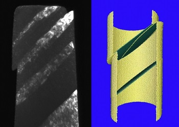
Experimental observation of coherent twin boundary (CTB) sliding in a nanopillar subjected to compression. (Courtesy of the researchers)
Some previous research suggested that these twin crystal boundaries are incapable of sliding due to the limited number of defects. Indeed, no experimental observations of such sliding have been reported before at room temperature. Now, a combination of theoretical analysis and experimental work reported in the Nature Communications paper has shown that in fact, under certain kinds of loads these grains can slide along the boundary. Understanding this property will be important for developing ways to engineer material properties to optimize them for specific applications, Dao says.
“A lot of high-strength nanocrystalline materials [with grains sizes measured in less than 100 nanometers] have low ductility and fatigue properties, and failure grows quite quickly with little stretching,” he says. Conversely, in the metals that incorporate CTBs, that “enhances the strength and preserves the good ductility.” But understanding how these materials behave when subjected to various mechanical stresses is important in order to be able to harness them for structural uses. For one thing, it means that the way the material deforms is quite uneven: Distortions in the direction of the planes of the CTBs can happen much more readily than in other directions.
The experiment was carried out with copper, but the results should apply to some other metals with similar crystal structures, such as gold, silver, and platinum. These materials are widely used in electronic devices, Dao says. “If you design these materials” with structures in the size range explored in this work, which involves features smaller than a few hundred nanometers across, “you need to be aware of these kinds of deformation modes.”
Molecular dynamics simulation showing coherent twin boundary (CTB) sliding in a nanopillar under compression. (Courtesy of the researchers)
The sliding, once understood, can be used for significant advantages. For example, researchers could design extremely strong nanostructures based on the known orientation dependence; or by knowing the type and direction of force that’s required to initiate the sliding, it might be possible to design a device that could be activated, such as an alarm, in response to a specific level of stress.
“This study confirmed CTB sliding, which was previously considered impossible, and its particular driving conditions,” says Zhiwei Shan, a senior co-author and dean of the School of Materials Science and Engineering at Xi’an Jiao Tong University in China. “Many things could become possible when previously unknown activation or enabling conditions are discovered.”
“This work has identified through both systematic experiments and analysis the occurrence of an important mechanical characteristic which is found only in certain special types of interfaces and at the nanoscale. Given that this phenomenon can potentially be applicable to a broad range of crystalline materials, one can envision new materials design approaches involving nanostructures to optimize a variety of mechanical and functional characteristics,” Suresh says.
“This discovery could fundamentally change our understanding of plastic deformation in nanotwinned metals and should be of broad interest to the material research community,” says Huajian Gao, the Walter H. Annenberg Professor of Engineering at Brown University, who was not involved in this work.
Gao adds that “CTBs are key to engineering novel nanotwinned materials with superior mechanical and physical properties such as strength, ductility, toughness, electrical conductivity, and thermal stability. This paper significantly advances our knowledge in this field by revealing large-scale sliding of CTBs.”
The team included researchers at Xi’an Jiaotong University in China, Johns Hopkins University in Baltimore, the Chinese Academy of Sciences in China, and Nanyang Technological University in Singapore. The work was supported by the Natural Science Foundation of China, the National Science Foundation, the U.S. Department of Energy, and the Singapore-MIT Alliance.
Share on:


Testimonial
"We’re proud to call I-Connect007 a trusted partner. Their innovative approach and industry insight made our podcast collaboration a success by connecting us with the right audience and delivering real results."
Julia McCaffrey - NCAB GroupSuggested Items
Trouble in Your Tank: Implementing Direct Metallization in Advanced Substrate Packaging
09/15/2025 | Michael Carano -- Column: Trouble in Your TankDirect metallization systems based on conductive graphite are gaining popularity throughout the world. The environmental and productivity gains achievable with this process are outstanding. Direct metallization reduces the costs of compliance, waste treatment, and legal issues related to chemical exposure. A graphite-based direct plate system has been devised to address these needs.
Closing the Loop on PCB Etching Waste
09/09/2025 | Shawn Stone, IECAs the PCB industry continues its push toward greener, more cost-efficient operations, Sigma Engineering’s Mecer System offers a comprehensive solution to two of the industry’s most persistent pain points: etchant consumption and rinse water waste. Designed as a modular, fully automated platform, the Mecer System regenerates spent copper etchants—both alkaline and acidic—and simultaneously recycles rinse water, transforming a traditionally linear chemical process into a closed-loop system.
Driving Innovation: Depth Routing Processes—Achieving Unparalleled Precision in Complex PCBs
09/08/2025 | Kurt Palmer -- Column: Driving InnovationIn PCB manufacturing, the demand for increasingly complex and miniaturized designs continually pushes the boundaries of traditional fabrication methods, including depth routing. Success in these applications demands not only on robust machinery but also sophisticated control functions. PCB manufacturers rely on advanced machine features and process methodologies to meet their precise depth routing goals. Here, I’ll explore some crucial functions that empower manufacturers to master complex depth routing challenges.
Trouble in Your Tank: Minimizing Small-via Defects for High-reliability PCBs
08/27/2025 | Michael Carano -- Column: Trouble in Your TankTo quote the comedian Stephen Wright, “If at first you don’t succeed, then skydiving is not for you.” That can be the battle cry when you find that only small-diameter vias are exhibiting voids. Why are small holes more prone to voids than larger vias when processed through electroless copper? There are several reasons.
The Government Circuit: Navigating New Trade Headwinds and New Partnerships
08/25/2025 | Chris Mitchell -- Column: The Government CircuitAs global trade winds continue to howl, the electronics manufacturing industry finds itself at a critical juncture. After months of warnings, the U.S. Government has implemented a broad array of tariff increases, with fresh duties hitting copper-based products, semiconductors, and imports from many nations. On the positive side, tentative trade agreements with Europe, China, Japan, and other nations are providing at least some clarity and counterbalance.