


 Trouble in Your Tank: Implementing Direct Metallization in Advanced Substrate Packaging
 It’s Only Common Sense: Storytelling That Sells—Stop Pitching, Start Painting Pictures
 The Right Approach: Get Ready for ISO 9001 Version 6


Atotech Presents a Novel E’Less Copper and Blackening Process for Touchscreen Application at the Eurodisplay 2017
November 1, 2017 | AtotechEstimated reading time: 2 minutes
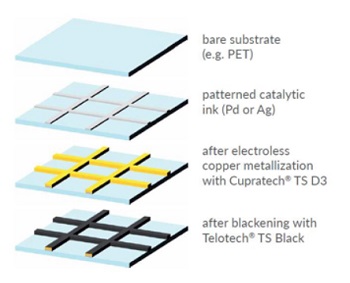
Atotech is one of the world’s leading manufacturers of specialty chemicals and equipment for the printed circuit board, IC-substrate and semiconductor industries, as well as for the decorative and functional surface finishing industries. As touchscreens become higher in demand and traditional build-up technology based on vapor deposited Indium Tin Oxide (ITO) reach its limitations, the new metal mesh technology to produce the sensor grid for advanced touch screens and sensors finds its momentum. While ITO has a low conductivity and is a brittle material, copper meshes feature a low resistance – ideal for use in large displays – coupled with the mechanical properties required for flexible or curved touch screens.
Visitors to the Eurodisplay 2017 are invited to learn more about this novel, additive and ITO free process for the formation of metal mesh and TFT electrodes.
When: Thursday, November 2, at 3:40pm
Where: Berlin, Melia Hotel, Friedrichstraße 103
Presenter: Roger Massey, Business Development Manager at Atotech GmbH
Cupratech TS D3 and Telotech® TS Black – Solutions for fully additive processing of Cu mesh touch sensors
Cupratech TS D3
Atotech’s metallization specialists have developed a new and tailor-made electroless copper process which allows the full additive build-up of copper meshes based on catalytic palladium or silver layers. “Cupratech® TS D3 features quick initiation and a high deposition rate of up to 140 nm/min for a minimized attack on the conductor tracks,” states Lars-Eric Pribyl, Global Product Manager Desmear and Metallization at Atotech Deutschland GmbH. “The process deposits a fine grain copper layer with high conductivity over the entire sensor. It is mass production proven and has been optimized to enable an excellent track shape.”
Telotech TS Black
Touch sensors are used in applications where the user does not want to see the conductor tracks within their display. “With Telotech TS Black, Atotech has developed a unique blackening process that greatly reduces the visibility of copper conductors on transparent substrates like PET,” continues Pribyl. “The process features very mild process conditions and provides a uniform black/dark finish to copper structures and surfaces. Like Cupratech TS D3, Telotech TS Black is applied in horizontal or reel-to-reel manufacturing equipment.”
Eurodisplay will be held from October 31 to November 2, 2017, in Berlin, Germany and discusses the latest development in all types of displays, electronics, and their impact on society.
About Atotech
Atotech is one of the world’s leading manufacturers of specialty chemicals and equipment for the printed circuit board, IC-substrate and semiconductor industries, as well as for the decorative and functional surface finishing industries. Atotech has annual sales of USD1.1 billion. The company is fully committed to sustainability – we develop technologies to minimize waste and to reduce environmental impact. Atotech has its headquarters in Berlin, Germany, and employs more than 4,000 people in over 40 countries.
Share on:


Testimonial
"The I-Connect007 team is outstanding—kind, responsive, and a true marketing partner. Their design team created fresh, eye-catching ads, and their editorial support polished our content to let our brand shine. Thank you all! "
Sweeney Ng - CEE PCBSuggested Items
Trouble in Your Tank: Implementing Direct Metallization in Advanced Substrate Packaging
09/15/2025 | Michael Carano -- Column: Trouble in Your TankDirect metallization systems based on conductive graphite are gaining popularity throughout the world. The environmental and productivity gains achievable with this process are outstanding. Direct metallization reduces the costs of compliance, waste treatment, and legal issues related to chemical exposure. A graphite-based direct plate system has been devised to address these needs.
Closing the Loop on PCB Etching Waste
09/09/2025 | Shawn Stone, IECAs the PCB industry continues its push toward greener, more cost-efficient operations, Sigma Engineering’s Mecer System offers a comprehensive solution to two of the industry’s most persistent pain points: etchant consumption and rinse water waste. Designed as a modular, fully automated platform, the Mecer System regenerates spent copper etchants—both alkaline and acidic—and simultaneously recycles rinse water, transforming a traditionally linear chemical process into a closed-loop system.
Driving Innovation: Depth Routing Processes—Achieving Unparalleled Precision in Complex PCBs
09/08/2025 | Kurt Palmer -- Column: Driving InnovationIn PCB manufacturing, the demand for increasingly complex and miniaturized designs continually pushes the boundaries of traditional fabrication methods, including depth routing. Success in these applications demands not only on robust machinery but also sophisticated control functions. PCB manufacturers rely on advanced machine features and process methodologies to meet their precise depth routing goals. Here, I’ll explore some crucial functions that empower manufacturers to master complex depth routing challenges.
Trouble in Your Tank: Minimizing Small-via Defects for High-reliability PCBs
08/27/2025 | Michael Carano -- Column: Trouble in Your TankTo quote the comedian Stephen Wright, “If at first you don’t succeed, then skydiving is not for you.” That can be the battle cry when you find that only small-diameter vias are exhibiting voids. Why are small holes more prone to voids than larger vias when processed through electroless copper? There are several reasons.
The Government Circuit: Navigating New Trade Headwinds and New Partnerships
08/25/2025 | Chris Mitchell -- Column: The Government CircuitAs global trade winds continue to howl, the electronics manufacturing industry finds itself at a critical juncture. After months of warnings, the U.S. Government has implemented a broad array of tariff increases, with fresh duties hitting copper-based products, semiconductors, and imports from many nations. On the positive side, tentative trade agreements with Europe, China, Japan, and other nations are providing at least some clarity and counterbalance.