


 Trouble in Your Tank: Implementing Direct Metallization in Advanced Substrate Packaging
 It’s Only Common Sense: Storytelling That Sells—Stop Pitching, Start Painting Pictures
 The Right Approach: Get Ready for ISO 9001 Version 6


Folding Circuits Just Atoms Thick Using the Principles of Origami
November 2, 2017 | AVS: Science and Technology of Materials, Interfaces, and ProcessingEstimated reading time: 2 minutes
While the creation of a paper swan using origami may be intriguing, the idea of creating 3-D circuits based on similar design principles is simply mindboggling. Researchers have focused on large scale synthesis and device fabrication using ultra-thin materials, which has led to improvements in 2-D models and the introduction of 3-D vertically integrated devices.
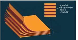
A new method allows scientists to craft individual tiny films, each just a few atoms high, and stack them for new kinds of electronics. Credit: Luis Ibarra, University of Chicago Creative
Origami, the well-known Japanese art of paper folding, generates complex 3-D structures from flat 2-D paper. While the creation of a paper swan may be intriguing, the idea of creating 3-D circuits based on similar design principles is simply mindboggling. This science fiction-sounding research is a project that Jiwoong Park and colleagues from the University of Chicago have been developing over the last few years.
Park's focus on large scale synthesis and device fabrication using ultra-thin materials has led to improvements in 2-D models and the introduction of 3-D vertically integrated devices.
Using atomically thin materials, Park synthesizes large scale integrated circuits that can be stitched together laterally to form a 2-D module. In their most recent project, his team has vertically integrated these 2-D modules to produce 3-D stacks.
Circuits have traditionally been developed using bulky substrate platforms, like silicon, and until recently were unable to function independently. Circuits based only on atomically thin materials liberate research from these conventional limitations. Combining various ultra-thin building blocks also allows for the integration of different electric and thermal properties within the same circuit, exponentially increasing functionality.
"For our research, we first generate atomically thin paper with different color[s] representing different electrical, optical, or thermal properties. We combine them in the lateral direction, equivalent to stitching. We stack them on top of one another, which is vertical integration. By doing so we are trying to develop large scale, fully functioning integrated circuits using these atomically thin materials as 2-D building blocks or color paper," Park said.
The use of these ultra-thin materials, as opposed to typical components and resources, allows for a smaller circuit, but surprisingly not one that is microscopically small and therefore difficult to manipulate. The 2-D ingredients are assembled in such a way that they can be viewed with a simple optical microscope or even with the naked eye and can be handled accordingly.
Potential applications of this technology are also extensive. Similar to the way folding is applicable in objects used in day-to-day life, such as umbrellas or parachutes, integrated circuits would be able to contain a large surface area in a relatively condensed volume. Functionality in this context could be applied to a diverse set of new devices using the capabilities of condensed circuitry.
"What we are interested in developing is this mechanism of taking all these surfaces and device elements and folding them into tight spaces. Upon our cue, we want them to deploy to really large functioning surfaces," Park said.
Share on:


Testimonial
"The I-Connect007 team is outstanding—kind, responsive, and a true marketing partner. Their design team created fresh, eye-catching ads, and their editorial support polished our content to let our brand shine. Thank you all! "
Sweeney Ng - CEE PCBSuggested Items
September 2025 PCB007 Magazine: The Future of Advanced Materials
09/16/2025 | I-Connect007 Editorial TeamMoore’s Law is no more, and the advanced material solutions being developed to grapple with this reality are surprising, stunning, and perhaps a bit daunting. Buckle up for a dive into advanced materials and a glimpse into the next chapters of electronics manufacturing.
I-Connect007 Launches Advanced Electronics Packaging Digest
09/15/2025 | I-Connect007I-Connect007 is pleased to announce the launch of Advanced Electronics Packaging Digest (AEPD), a new monthly digital newsletter dedicated to one of the most critical and rapidly evolving areas of electronics manufacturing: advanced packaging at the interconnect level.
Panasonic Industry will Double the Production Capacity of MEGTRON Multi-layer Circuit Board Materials Over the Next Five Years
09/15/2025 | Panasonic Industry Co., Ltd.Panasonic Industry Co., Ltd., a Panasonic Group company, announced plans for a major expansion of its global production capacity for MEGTRON multi-layer circuit board materials today. The company plans to double its production over the next five years to meet growing demand in the AI server and ICT infrastructure markets.
Trouble in Your Tank: Implementing Direct Metallization in Advanced Substrate Packaging
09/15/2025 | Michael Carano -- Column: Trouble in Your TankDirect metallization systems based on conductive graphite are gaining popularity throughout the world. The environmental and productivity gains achievable with this process are outstanding. Direct metallization reduces the costs of compliance, waste treatment, and legal issues related to chemical exposure. A graphite-based direct plate system has been devised to address these needs.
Fresh PCB Concepts: Designing for Success at the Rigid-flex Transition Area
08/28/2025 | Team NCAB -- Column: Fresh PCB ConceptsRigid-flex PCBs come in all shapes and sizes. Manufacturers typically use fire-retardant, grade 4 (FR-4) materials in the rigid section and flexible polyimide materials in the flex region. Because of the small size, some rigid-flex PCBs, like those for hearing aid devices, are among the most challenging to manufacture. However, regardless of its size, we should not neglect the transition area between the rigid and flexible material.