


 Trouble in Your Tank: Implementing Direct Metallization in Advanced Substrate Packaging
 It’s Only Common Sense: Storytelling That Sells—Stop Pitching, Start Painting Pictures
 The Right Approach: Get Ready for ISO 9001 Version 6


A Microscope for Magnetic Atoms
November 7, 2017 | ETH ZurichEstimated reading time: 3 minutes
Scanning tunnelling microscopes can make individual atoms of a material visible. Researchers at ETH Zurich have now also measured their magnetization using such a microscope. The new technology could be used in magnetic imaging as well as in magnetic information processing.
Philosophers in ancient Greece already believed that matter is made up of atoms. Only about 35 years ago, however, were atoms actually observed for the first time – in Zurich. The scanning tunnelling microscope developed by Gerd Binnig and Heinrich Rohrer allowed surfaces of materials to be investigated with a spatial resolution of less than one nanometre – enough to see individual atoms.
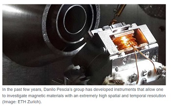
A team of researchers led by Urs Ramsperger and Danilo Pescia at the Laboratory for Solid State Physics of the ETH Zurich, together with a colleague at Istanbul Technical University, have now added a crucial detail to the capabilities of such extreme-resolution microscopes. As reported in the journal Scientific Reports, they succeeded in measuring the magnetization of a material with a spatial resolution of a few nanometres. In the future, this technology could be used for the magnetic imaging of materials as well as for the development of novel methods in information processing.
A technology that shouldn’t exist
The main peculiarity of the new technology is that, actually, it shouldn’t work at all. To resolve individual atoms, a scanning tunnelling microscope uses a metal tip that is put extremely close to the surface of a material, in fact to within the size of an atom (smaller than one nanometre). According to the rules of quantum mechanics, at such short distances electrons can tunnel from the metal tip into the material and thus create an electric current that can be used to create an image of the surface. The researchers at ETH now increased that distance to several nanometres and were doubly surprised, as Danilo Pescia explains: “On the one hand, despite the larger distance we still had very good spatial resolution, and on the other hand we were able to extract electrons from the tunnel region – although calculations had shown that extraction should be practically impossible.” Normally electrons tunnelling from the metal tip into the material, even at tip-surface separations of a few nanometres, are trapped in the gap in between and, according to theory, should leave the tunnel region only very rarely.
Information in the electron spin
The extracted electrons, however, contain valuable information. Their spin is particularly interesting to the researchers, as it tells them whether and in which direction the atoms of the material under investigation are magnetized. The spin designates an inner rotation of the electrons, but in practice only leads to a very small measurable signal. Detecting it is, therefore, a big technical challenge, particularly under the difficult conditions of a tunnelling experiment.
In their experiment, the scientists applied a suitable voltage to the metal tip of a scanning tunnelling microscope that caused electrons without a particular spin direction to be ejected. When they encountered magnetic atoms – atoms, that is, that have a well-defined spin – the spin direction of the atoms was transferred to the electrons extracted from the tunnel region. The spin direction of the extracted electrons was finally measured, using a spin detector. In this way, it was possible to detect the magnetization of the material with a spatial resolution of five nanometres.
Early attempts failed
Already around thirty years ago, a similar experiment was attempted both at IBM Zurich and at the National Institute of Standards and Technology in the USA. The goal of obtaining a spatially resolved image of the magnetic state, however, was not achieved. The researchers at ETH are satisfied that they now succeeded in spite of the negative predictions. Currently they are trying to understand their unexpected success theoretically, too, and also to push the limits of the newly developed technology. In the USA there is also a renewed interest in instruments similar to the one now built at ETH, and the National Science foundation provides generous funding for related projects.
Possibility of various applications
For Urs Ramsperger and Danilo Pescia, there is a clear lesson to be learned from this story: “In research one mustn’t be afraid of trying the impossible once in a while”, they say and add: “Sometimes things work better in practice than in theory – after all, paper is just paper.” Their courage has now been rewarded and will, the researchers hope, lead to various applications. For instance, the magnetic properties of materials could be studied in real time with a resolution of a trillionth of a second. As the current experiment effectively converted an electric voltage into a spin (which makes it an example of modern “spintronics”), the controlled manipulation of the magnetization of individual atoms should also be possible.
Share on:


Testimonial
"Our marketing partnership with I-Connect007 is already delivering. Just a day after our press release went live, we received a direct inquiry about our updated products!"
Rachael Temple - AlltematedSuggested Items
Altair, Wichita State University’s NIAR Sign MoU to Accelerate Aerospace Innovation
09/16/2025 | AltairAltair, a global leader in computational intelligence, and Wichita State University’s (WSU) National Institute for Aviation Research (NIAR), one of the world’s leading aerospace research institutions, have signed a memorandum of understanding (MoU) to advance innovation across the aerospace and defense industries.
AI-Powered Wearables Transform How Consumers Interact with Everyday Technology
09/15/2025 | PR NewswireThe global demand for AI-driven, touchless wearable technologies is accelerating as consumers seek more natural, seamless and intuitive ways to interact with their devices. Traditional touch screens and voice assistants, while effective, are increasingly viewed as limiting in a world where multitasking, mobility and efficiency are key. As industries from consumer electronics to augmented reality and enterprise computing embrace the possibilities of gesture-based control, the market for neural interfaces is rapidly expanding
Hanwha Aerospace to Collaborate with BAE Systems on Advanced Anti-jamming GPS for Guided Missiles
09/15/2025 | HanwhaHanwha Aerospace has signed a contract with BAE Systems to integrate next-generation, anti-jamming Global Positioning System (GPS) technology into Hanwha Aerospace’s Deep Strike Capability precision-guided weapon system.
United Electronics Corporation Unveils Revolutionary CIMS Galaxy 30 Automated Optical Inspection System
09/11/2025 | United Electronics CorporationUnited Electronics Corporation (UEC) today announced the launch of its new groundbreaking CIMS Galaxy 30 Automated Optical Inspection (AOI) machine, setting a new industry standard for precision electronics manufacturing quality control. The Galaxy 30, developed and manufactured by CIMS, represents a significant leap forward in inspection technology, delivering exceptional speed improvements and introducing cutting-edge artificial intelligence capabilities.
Intel Announces Key Leadership Appointments to Accelerate Innovation and Strengthen Execution
09/09/2025 | Intel CorporationIntel Corporation today announced a series of senior leadership appointments that support the company’s strategy to strengthen its core product business, build a trusted foundry, and foster a culture of engineering across the business.