


 Trouble in Your Tank: Implementing Direct Metallization in Advanced Substrate Packaging
 It’s Only Common Sense: Storytelling That Sells—Stop Pitching, Start Painting Pictures
 The Right Approach: Get Ready for ISO 9001 Version 6


Semiconductors with an Aligned Interface
November 13, 2017 | KAUSTEstimated reading time: 2 minutes
The electronic characteristics of an interface between two wide bandgap semiconductors are determined by researchers at KAUST, providing an insight that will help improve the efficiency of light-emitting and high-power electronic devices.
Semiconductors, such as silicon and gallium nitride, have electrical properties somewhere in between those of a conductor and an insulator. They only allow current to flow when electrons have enough energy to overcome a barrier known as bandgap. The bandgap—which may be direct or indirect, narrow or large—determines the properties of semiconductors and their consequent applications.
Materials with a large bandgap, for example, are useful in high-power electronics because they have larger breakdown voltage for energy-efficient transistors as compared with narrow bandgap materials, such as silicon. They can also produce light deep into the ultraviolet part of the spectrum, making them useful for disinfection and water purification.
These materials can be further tailored to a specific application by layering different semiconductors on top of each other to create a so-called heterostructure with the desired properties. But it is vital to understand how the bandgaps of two semiconductors align when semiconductors are brought together in this way.
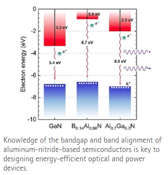
Haiding Sun and principle investigator Xiaohang Li from KAUST and coworkers from the Georgia Institute of Technology, USA, report that they experimentally measured the alignment of two emerging large bandgap materials: boron aluminum nitride and aluminum gallium nitride.
The 2014 Nobel Prize for physics was awarded in recognition of the development of gallium nitride light-emitting diodes. But, compared to gallium nitride, aluminum nitride has a much larger bandgap of 6.1 electronvolts. Its electronic properties can be tuned by replacing some of the aluminum atoms in the crystal with either boron or gallium.
The team created an interface between boron aluminum nitride with a boron to aluminum atom ratio of 14:86 and aluminum gallium nitride with a gallium nitride ratio of 30:70 on an aluminum-nitride-covered sapphire substrate.
They used high-resolution X-ray photoemission spectroscopy to measure the offset between the top and the bottom of the two material's bandgaps. They show that the bandgaps have a staggered alignment, with both the top and bottom edge of the bandgap of the Al0.7Ga0.3N lower than the respective edge in B0.14Al0.86N.
“Based on the experimental results, we can achieve a much higher amount of two-dimensional electron gas sheet carrier concentration in such junction,” says Sun. “The determination of the band alignment of B0.14Al0.86N/Al0.7Ga0.3N heterojunction provides valuable support in the design of optical and electronic devices based on such junctions.”
Share on:


Testimonial
"Advertising in PCB007 Magazine has been a great way to showcase our bare board testers to the right audience. The I-Connect007 team makes the process smooth and professional. We’re proud to be featured in such a trusted publication."
Klaus Koziol - atgSuggested Items
September 2025 PCB007 Magazine: The Future of Advanced Materials
09/16/2025 | I-Connect007 Editorial TeamMoore’s Law is no more, and the advanced material solutions being developed to grapple with this reality are surprising, stunning, and perhaps a bit daunting. Buckle up for a dive into advanced materials and a glimpse into the next chapters of electronics manufacturing.
I-Connect007 Launches Advanced Electronics Packaging Digest
09/15/2025 | I-Connect007I-Connect007 is pleased to announce the launch of Advanced Electronics Packaging Digest (AEPD), a new monthly digital newsletter dedicated to one of the most critical and rapidly evolving areas of electronics manufacturing: advanced packaging at the interconnect level.
Panasonic Industry will Double the Production Capacity of MEGTRON Multi-layer Circuit Board Materials Over the Next Five Years
09/15/2025 | Panasonic Industry Co., Ltd.Panasonic Industry Co., Ltd., a Panasonic Group company, announced plans for a major expansion of its global production capacity for MEGTRON multi-layer circuit board materials today. The company plans to double its production over the next five years to meet growing demand in the AI server and ICT infrastructure markets.
Trouble in Your Tank: Implementing Direct Metallization in Advanced Substrate Packaging
09/15/2025 | Michael Carano -- Column: Trouble in Your TankDirect metallization systems based on conductive graphite are gaining popularity throughout the world. The environmental and productivity gains achievable with this process are outstanding. Direct metallization reduces the costs of compliance, waste treatment, and legal issues related to chemical exposure. A graphite-based direct plate system has been devised to address these needs.
Fresh PCB Concepts: Designing for Success at the Rigid-flex Transition Area
08/28/2025 | Team NCAB -- Column: Fresh PCB ConceptsRigid-flex PCBs come in all shapes and sizes. Manufacturers typically use fire-retardant, grade 4 (FR-4) materials in the rigid section and flexible polyimide materials in the flex region. Because of the small size, some rigid-flex PCBs, like those for hearing aid devices, are among the most challenging to manufacture. However, regardless of its size, we should not neglect the transition area between the rigid and flexible material.