


 Trouble in Your Tank: Implementing Direct Metallization in Advanced Substrate Packaging
 It’s Only Common Sense: Storytelling That Sells—Stop Pitching, Start Painting Pictures
 The Right Approach: Get Ready for ISO 9001 Version 6


Electronics and Optics on One Chip Getting Light out of Silicon
November 13, 2017 | University of TwenteEstimated reading time: 2 minutes
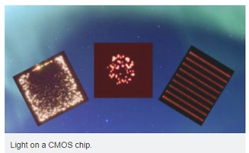
Electronics and light don't go well together on a standard 'CMOS' chip. Researcher Satadal Dutta of the University of Twente succeeded in introducing a light connection into the heart of a semiconductor chip. In this way, two circuits can communicate. Or: the worlds of electronics and photonics are connected.
What is particularly attractive about Dutta's solution is that no special materials or manufacturing processes are needed: the light comes from silicon. The light source, detector and the light channel can be made using the technology that is used to make the electronic circuits. Fully optical circuits are available nowadays, but they use materials like indium phosphide and gallium arsenide, which can't easily be combined with the CMOS chip processes used for semiconductor chips you'll find in today's smartphones, for example.
Avalanche LED
The alternative would be: make a LED out of silicon. And that's the problem: silicon only emits a tiny amount of infrared light, while a detector made out of silicon needs visible light. They are talking and listening at different wavelengths. Dutta therefore chooses a remarkable way out: connect the LED reverse. At low voltages, there's no current, but at a voltage that is high enough, there will be a small current that amplifies itself like an avalanche. In this 'avalanche mode', the LED will transmit visible light. Using the same process, the light detector, as well as the light channel in-between can be made. Thanks to the special comb structure that Dutta designed, the light source gets more uniform and energy efficient.
Isolation
An optical link on a chip is a good way to 'galvanically' isolate two circuits from each other. This is often necessary in cases where one circuit is a low-voltage and low-current one, while the other is a high-power circuit. They should be connected, but not by conducting wires, for reasons of safety. A classic transformer is an option then, but an optical connection is often used as well. Until now, this is a separate 'optocoupler', which is large and has a limited bit rate. Dutta's new solution is much more compact as an alternative: it total, it is just a few tens of microns and it offers the protection that's needed. Compared to optical channels in full-optical circuits, the energy consumption is relatively high, as there is quite some scattering of light. On the other hand: designing the electronics around the optical link in an efficient way, the amount of light needed for a successful connection, can be kept to a minimum.
Connecting worlds
All-optical circuits may become the 'new electronics', predictions say. In the transition from electronic to optic circuits, hybrid circuits, like the one Dutta designed, could play an important role.
Satadal Dutta (1990, Barrackpore, India) did his PhD research in the Semiconductor Components group of Prof Jurriaan Schmitz, together with the Integrated Circuit Design group of Prof. Bram Nauta. Dutta defended his thesis 'Avalanche-mode silicon LEDs for monolithic optical coupling in CMOS technology' on 8 November. It was supported financially by NWO-TTW in The Netherlands and by NXP Semiconductors.
Share on:


Testimonial
"We’re proud to call I-Connect007 a trusted partner. Their innovative approach and industry insight made our podcast collaboration a success by connecting us with the right audience and delivering real results."
Julia McCaffrey - NCAB GroupSuggested Items
TTCI and The Training Connection Strengthen Electronics Manufacturing with Test Services and Training at PCB West 2025
09/16/2025 | The Test Connection Inc.The Test Connection Inc. (TTCI), a trusted provider of electronic test and manufacturing solutions, and The Training Connection LLC (TTC-LLC) will exhibit at PCB West 2025, taking place Wednesday, October 1, 2025, at the Santa Clara Convention Center in California. Visitors are invited to Booth 113 to explore the companies’ complementary expertise in test engineering services and workforce development for the electronics industry.
Beyond the Board: What Companies Need to Know Before Entering the MilAero PCB Market
09/16/2025 | Jesse Vaughan -- Column: Beyond the BoardThe MilAero electronics supply chain offers opportunities for manufacturers that are both prestigious and strategically important. Serving prime contractors and Tier-1 suppliers can mean long-term program stability and the satisfaction of contributing to national security. At the same time, this sector is unlike commercial electronics in almost every respect. Success requires more than technical capabilities, it requires patience, preparation, attention to detail, and a clear understanding of how the business model differs.
India’s Aerospace and Defence Engineered for Power, Driven by Electronics
09/16/2025 | Gaurab Majumdar, Global Electronics AssociationWith a defence budget of $82.05 billion (2025–26) and a massive $223 billion earmarked for aerospace and defence spending over the next decade, India is rapidly positioning itself as a major player in the global defence and aerospace market.
I-Connect007 Launches Advanced Electronics Packaging Digest
09/15/2025 | I-Connect007I-Connect007 is pleased to announce the launch of Advanced Electronics Packaging Digest (AEPD), a new monthly digital newsletter dedicated to one of the most critical and rapidly evolving areas of electronics manufacturing: advanced packaging at the interconnect level.
Global Interposer Market to Surge Nearly Fivefold by 2034
09/15/2025 | I-Connect007 Editorial TeamRevenue for the global interposer market is projected to climb from $471 million in 2025 to more than $2.3 billion by 2034, according to a new report from Business Research Insights. The growth represents a CAGR of nearly 20 percent over the forecast period.